CIDAN-XE: Computing in DRAM with Artificial Neurons
 Gian Singh
 Ankit Wagle1
  Sarma Vrudhula
- 1School of Computing and Augmented Intelligence, Arizona State University, Tempe, AZ, United States
- 2Department of Electrical and Computer Engineering, Texas A&M University, College Station, TX, United States
This paper presents a DRAM-based processing-in-memory (PIM) architecture, called CIDAN-XE. It contains a novel computing unit called the neuron processing element (NPE). Each NPE can perform a variety of operations that include logical, arithmetic, relational, and predicate operations on multi-bit operands. Furthermore, they can be reconfigured to switch operations during run-time without increasing the overall latency or power of the operation. Since NPEs consume a small area and can operate at very high frequencies, they can be integrated inside the DRAM without disrupting its organization or timing constraints. Simulation results on a set of operations such as AND, OR, XOR, addition, multiplication, etc., show that CIDAN-XE achieves an average throughput improvement of 72X/5.4X and energy efficiency improvement of 244X/29X over CPU/GPU. To further demonstrate the benefits of using CIDAN-XE, we implement several convolutional neural networks and show that CIDAN-XE can improve upon the throughput and energy efficiency over the latest PIM architectures.
1 Introduction
The continuing exponential growth in the number of electronic systems that access the internet combined with an increasing emphasis on data analytics is giving rise to applications that continuously process terabytes of data. The latency and energy consumption of such data-intensive or data-centric (Gokhale et al., 2008) applications is dominated by the movement of the data between the processor and memory. In modern systems about 60% of the total energy is consumed by the data movement over the limited bandwidth channel between the processor and memory (Boroumand et al., 2018).
The recent growth of data-intensive applications is due to the proliferation of machine learning techniques which are most often implemented using convolutional/deep neural networks (CNNs/DNNs) (Angizi et al., 2019). CNNs/DNNs are large computation graphs with huge storage requirements. For instance even an old neural network such as VGG-19 (Simonyan and Zisserman, 2015) consists of 19 layers, has about 144 million parameters, and performs about 19.6 billion operations. Almost all of the neural networks used today are much larger than VGG-19 (Dai et al., 2021). These large computation graphs are evaluated in massive data centers that house millions of high-performance servers with arrays of multi-core CPUs and GPUs. For instance, to process one image using the VGG-19 network, a TITAN X GPU takes about 2.35 s, consumes about 5 Joules of energy, and operates at about 228 W of power (Li et al., 2016). Other data-intensive applications include large scale encryption/decryption programs (Myers, 1999), large-scale graph processing (Angizi and Fan, 2019a), bio-informatics (Huangfu et al., 2019), to name just a few. Each transaction over the memory channel consumes about three orders magnitude greater energy than executing a floating-point operation on the processor and requires almost two orders of magnitude greater latency than accessing the on-chip cache (Dally, 2015). Thus the present approach to executing data-intensive applications using CPUs and GPUs is fast becoming unsustainable, both in terms of their limited performance and high energy consumption.
One approach to circumvent the processor-memory bottleneck is known as processing-in-memory (PIM). The dominant choice of memory in PIM is DRAM due to its large capacity (tens to hundreds of gigabytes) and the high degree of parallelism it offers because a single DRAM command can operate on an entire row containing kilobytes of data. The main idea in PIM is to perform computations within the DRAM directly without involving the CPU. Only the control signals are exchanged between the processor and the off-chip memory indicating the start and the end of the operation. This leads to a great reduction in data movement and can lead to orders of magnitude improvement in both throughput and energy efficiency as compared to traditional processors. For instance, the PIM architectures such as ReDRAM (Angizi and Fan, 2019b) are about 49X faster and consume about 21X less energy as compared to a processor with GPUs for graph analysis applications. Similarly, SIMDRAM (Hajinazar et al., 2021) is about 88X/5.8X faster and 257X/31X more energy efficient than a CPU/GPU for a set of 16 basic operations.
For the widespread adoption of the PIM using the DRAM platform, there must be minimum disruption to the memory array structure and the access protocol of DRAM. Being an extremely cost-sensitive market, DRAM fabrication processes are highly optimized to produce dense memories. The DRAM design and optimization requires very high levels of expertise in process technology, device physics, custom IC layout, and analog and digital design. Consequently, a PIM architecture that is non-intrusive—meaning that it does not interfere with the DRAM array or its timing—is paramount.
This paper describes, CIDAN-XE, a new PIM architecture that embeds new compute elements, which are referred to as neuron processing elements (NPE). The NPEs are embedded in the DRAM chip but reside outside the DRAM array. CIDAN-XE increases the computation capability of the memory without sacrificing its area, changing its access protocol, or violating any timing constraints. Each NPE consists of a small collection of artificial neurons (a.k.a. threshold logic gates (Muroga, 1971)) enhanced with local registers. The implementation of an artificial neuron is a mixed-signal circuit that computes a set of threshold functions of its inputs. The specific threshold function is selected on each cycle by enabling/disabling a subset of the inputs associated with the artificial neuron by control bits. This results in a negligible overhead for providing reconfigurability. In addition to the threshold functions, an NPE realizes some non-threshold functions by a sequence of artificial neuron evaluations. Furthermore, artificial neurons consume substantially less energy and are significantly smaller than their CMOS equivalent implementations (Wagle et al., 2019). Due to the inherent advantages of NPE in reconfigurability, its small area footprint, and low energy consumption, CIDAN-XE platform in this paper is shown to achieve high throughput and energy efficiency for several operations and CNN architectures.
The main contributions of the paper are listed below:
• This paper presents a novel integration of an artificial neuron processing element in a DRAM architecture to perform logic operations, arithmetic operations, relational operations, predication, and a few other complex operations under the timing and area constraints of the DRAM modules.
• The proposed design can process data with different element sizes (1-bit, 2-bits, 4-bits, 8-bits, 16-bits, and 32-bits) which are used in popular programming languages. This processing is enabled by using operand decomposition computing and scheduling algorithms for the NPE.
• A case study on CNN algorithm with optimized data-mapping on DRAM banks for improved throughput and energy efficiency under the limitations of existing DRAM access protocols and timing constraints is presented.
This paper is organized as follows. Section 2 lays down the background of DRAM organization, operations, and its timing constraints. Prior processing in-memory architectures are also explained in Section 2. Section 3 describes in detail the architecture of the neuron processing element (NPE) and its operations. Section 4 illustrates the top-level design of the architecture and its parallel operation under DRAM timing constraints. Section 5 presents the mapping and the implementation of CNN on CIDAN-XE. The experimental results and comparison with the commercial architectures and prior PIM architectures are presented in Section 6 and Section 7 concludes the paper.
Note: A preliminary version of this paper appeared in (Singh et al., 2021). The work reported herein extends (Singh et al., 2021) in several significant ways. First, the processing element used in the preliminary work could perform a very limited set of functions, i.e. only bit-serial addition, comparison, and basic logic operations since its structure only contained a single neuron. However, the proposed processing element now supports larger and more complex functions such as accumulation, adder-tree, comparison, ReLU, etc. due to the presence of more neurons and the addition of local registers. While the preliminary work could only support bit-vector calculations, the proposed work supports more complex workloads such as CNNs.
2 Background
2.1 DRAM: Architecture, Operation and Timing Parameters
This subsection includes a description of the architecture, operation, and timing specifications of a DRAM. For in-memory computation, these specifications are needed to ensure that the area and timing of the original DRAM architecture are preserved when computation is integrated.
The conventional organization of DRAM is shown in Figure 1A. This organization consists of several levels of hierarchy. The lowest level of the hierarchy, which forms the building block of DRAM, is called a bank. A bank contains a 2D array of memory cells, a row of sense amplifiers, a row decoder, and a column decoder. A collection of banks is contained in a DRAM chip. Memory banks in a chip share the I/O ports and an output buffer, and hence, only one bank per chip can be accessed to read or write using a shared memory bus at a given time. DRAM chips are arranged on a circuit board module called Dual-in-line memory module (DIMM). A DIMM has DRAM chips arranged on its two sides (front and back). Each side is called a rank and is connected to a chip select signal. The ranks use the memory channel in a lockstep manner but they are independent and can operate in parallel. When data needs to be fetched from the DRAM, the CPU communicates with the DRAM over a memory channel with a data bus that is generally 64 bits wide. Multiple DIMMs can share a memory channel. Hence, a multiplexer is used to select the DIMM to provide data to the CPU. One rank of the DIMM provides data to fill the entire data bus. Note that all the DRAM chips in a rank operate simultaneously while reading or writing data. The memory hierarchy presented above is meant to activate several parts of the DRAM in parallel and fetch large chunks of data simultaneously from multiple banks in a single cycle. By extension, in-memory architectures use this hierarchy to perform operations on large segments of data in parallel.
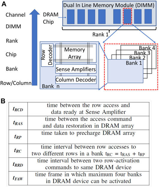
FIGURE 1. (A) Top-level DRAM architecture and (B) Important Timing Constraints of DRAM.
A DRAM memory controller controls the data transfers between the DRAM and the CPU. Therefore, almost all the currently available in-memory architectures (Li et al., 2017; Seshadri et al., 2017; Deng et al., 2018; Angizi and Fan, 2019b; Hajinazar et al., 2021) modify the technique used to access the data and extend the functionality of the memory controller to perform the logic operations. The controller issues a sequence of three commands to the DRAM: Activate (ACT), Read/Write (R/W), and precharge (PRE), along with the memory address. The ACT command copies a row of data into the sense amplifiers through the corresponding bitlines. Here, the array of sense amplifiers is called a row buffer as it holds the data until another row is activated in the bank. The READ/WRITE command reads/writes a subset of row buffer to/from the data bus by using a column decoder. After the data is read or written, the PRE command charges the bitlines to its resting voltage
Due to the power budget, traditional DRAM architectures allow only four banks in a DRAM chip to stay activated simultaneously within a time frame of tFAW. The DRAM controller can issue two consecutive ACT commands to different banks separated by a time period of tRRD. As a reference, a 1 Gb DDR3-1600 RAM has tRRD = 7.5ns and tFAW = 30 ns (Chandrasekar et al., 2021). In Section 4 the impact of these timing parameters on the delay in executing logic functions will be shown for the proposed processing-in-memory (PIM) architecture.
2.2 Processing in Memory
PIM architectures are classified into two categories: mixed-signal PIM (mPIM) and digital PIM (dPIM) architectures. The dPIM architectures can be further classified as internal PIM (iPIM) and external PIM (ePIM). The differences between these architectures are described as follows.
The mPIM architectures use memory crossbar-arrays to perform matrix-vector multiplication (MVM) and accumulation in the analog domain. These architectures then convert the result into a digital value using an analog to digital converter (ADC). Thus mPIM architectures approximate the result, and accuracy depends on the precision of the ADC. A few representative works of mPIM are (Chi et al., 2016; Guo et al., 2017; Yin et al., 2020). mPIM architectures are based on either SRAMs or non-volatile memories. They are exclusively used for machine learning applications to perform multiply and accumulate (MAC) operations.
In contrast to the mPIM architecture, iPIM architectures (Li et al., 2017; Seshadri et al., 2017; Deng et al., 2018; Angizi and Fan, 2019b; Xin et al., 2020; Hajinazar et al., 2021) modify the structure of the DRAM cell, the row decoding logic and sense amplifiers in such a way that each cell can perform a one-bit or two-bit logic operation. Thus, primitive logic operations can be carried out on an entire row (8 KB) in parallel. Logic operations on multi-bit operands are performed in a bit-serial manner (Judd et al., 2016; Ali et al., 2020), which results in lower throughput for large bit-width operands, e.g., multiplication. These architectures generally achieve high energy efficiency on bit-wise operations as they operate directly on memory rows and process entire rows in parallel.
The ePIM architectures embed digital logic outside the DRAM memory array, but on the same die. These architectures work on the subset of the memory row and hence process fewer elements in parallel. The logic gates used in ePIM architectures are designed for multi-bit elements and implement a limited number of operations. Hence, they act as hardware accelerators with high throughput for specific applications. Recently, the DRAM makers SK-Hynix (He et al., 2020) and Samsung (Kwon et al., 2021) introduced 16-bit floating-point processing units inside the DRAM. ePIM architectures have a high area overhead and have to reduce the size of memory arrays to accommodate the added digital logic.
For accelerating, multiplication, and other non-linear functions at higher bit-widths of 8 and 16 bits, certain look-up table architectures have also been proposed recently (Deng et al., 2019; Ferreira et al., 2021; Sutradhar et al., 2022). These architectures store small lookup tables in DRAM for implementing complex exponential and non-linear functions in a single clock cycle.
Though the existing PIM architectures can deliver much higher throughput as compared to the traditional CPU/GPU architectures (Angizi and Fan, 2019b), their disadvantages include loss of precision (mPIM architectures), low energy efficiency and high area overhead (ePIM architectures), and low throughput on complex operations (iPIM architectures).
2.3 Prior Work on Logic Operations (iPIM) and Arithmetic Operations (ePIM) in DRAM
Currently available iPIM architectures such as AMBIT (Seshadri et al., 2017), ReDRAM (Angizi and Fan, 2019b), DRISA (Li et al., 2017), DrAcc (Deng et al., 2018) and SIMDRAM (Hajinazar et al., 2021 extend the operations of a standard DRAM to perform logic operations.
A representative diagram of AMBIT operation on three rows is shown in Figure 2A. In a normal DRAM operation, only one of the rows is activated and only one storage capacitor goes into the charge sharing phase with the corresponding bitline (precharged to
where δ is bitline deviation, Cc is the cell capacitance, Cb is the bitline capacitance, and k is the number of cells in fully charge state. For k = 2, 3, δ will be positive and the sense amplifier evaluates to 1, otherwise δ will be negative and the sense amplifier evaluates to 0. In this way, TRA performs a majority operation on three inputs. Since the rows remain connected to the BL, the original data in the capacitors is lost and overwritten by the result value on BL.
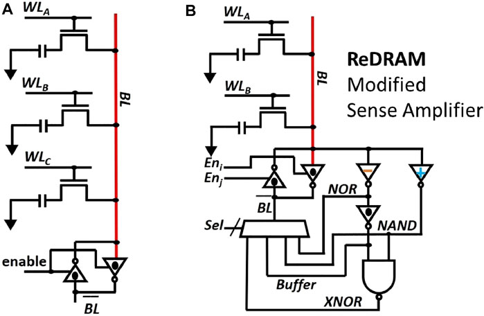
FIGURE 2. Prior work (iPIM). Hardware architecture of (A) AMBIT (Seshadri et al., 2017) and (B) ReDRAM (Angizi and Fan, 2019b)
In the case of ReDRAM, two rows are activated (double row activation (DRA)) simultaneously and they undergo the same charge sharing phase with the BL as in the case of AMBIT. To prevent the loss of original data at the end of TRA or DRA, both AMBIT and ReDRAM reserve some rows (referred to as compute rows) in the memory array to exclusively perform a logic operation. Hence, for every operation, the operands are copied from the source rows to the compute rows by using the copying operation described in (Seshadri et al., 2013). A copy operation is carried out by a command sequence of ACT → ACT → PRE which takes 82.5ns in 1 Gb DDR3-1600 (Chandrasekar et al., 2021). In AMBIT, all the 2-input operations such as AND, OR etc. are represented using a 3-input majority function.
ReDRAM improves upon the work by AMBIT by reducing the number of rows that need to be activated simultaneously to two. After the charge sharing phase between two rows, a modified sense amplifier is used to perform the logic operation and write back the result. The modified sense amplifier has inverters with different threshold voltages (switching voltages) to perform the logic operations as shown in Figure 2B. Each inverter enables the computation of a different logic function. A multiplexer is used to choose between one of the logic functions.
ReDRAM, AMBIT, and the related designs DRISA, DrAcc and SIMDRAM, have a complete set of basic functions and can exploit full internal bank data width with a minimum area overhead. However, their shortcomings include:
• These designs rely on sharing charges between the storage capacitors and bitlines for their operation. Due to the analog nature of the operation, the reliability of the operation can be effected under varying operating conditions.
• ReDRAM modifies the inverters in the sense amplifier to shift their switching points using transistors of varying threshold voltage at the design time. Hence, such a structure is also vulnerable to process variations.
• All these designs overwrite the source operands, because of which rows need to be copied before performing the logic operations. Such an operation reduces the overall throughput that can be achieved when performing the logic operations on bulk data.
Existing iPIM architectures perform bitwise operations which result in a significant latency and energy consumption for multi-bit (4-bits, 8-bits, 16-bits, etc.) operands. Hence, their throughput and energy benefits show a decreasing trend for higher bit precision. To overcome this shortcoming, the architectures with custom logic (large multipliers and accumulators) He et al., 2020), programmable computing units (Kwon et al., 2021), and LUT-based designs LAcc (Deng et al., 2019), pPIM (Sutradhar et al., 2022), pLUTo (Ferreira et al., 2021) have been proposed. These architectures embed external logic to the DRAM outside the memory array, hence, referred to as ePIM architectures. Such architectures are amenable to specific applications and act as hardware accelerators for them. The ePIM architectures have a huge area overhead and consequently sacrifice the DRAM storage capacity.
CIDAN-XE is designed to overcome the shortcomings of the discussed literature and provide flexibility to perform data-intensive applications with multi-bit operands. A comparison of CIDAN-XE with iPIM and ePIM architectures is shown in Table 1.
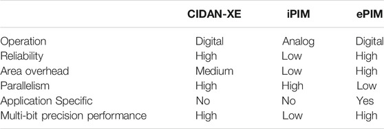
TABLE 1. Comparison of CIDAN-XE with iPIM and ePIM architectures.
Key Advantages of CIDAN-XE: The proposed platform, CIDAN-XE, improves the existing iPIM and ePIM architectures in seven distinct ways.
1. Neither the memory bank nor its access protocol is modified.
2. There is no need for special sense amplifiers for its operation.
3. The NPEs are DRAM fabrication process compatible and have a small area footprint.
4. There is no reduction in DRAM capacity.
5. CIDAN-XE adheres to the existing DRAM constraint of having a maximum of four active banks.
6. The NPEs connected to the DRAM do not rely on charge sharing over multiple rows and are essentially static logic circuits.
7. The NPEs are reconfigured at run-time using control bits to realize different functions and the cost of reconfiguration is negligible as compared to the LUT-based designs.
Further details are discussed in Section 3.
2.4 Threshold Logic Function and Artificial Neurons
A Boolean function f(x1, x2, …, xn) is called a threshold function if there exist weights wi for i = 1, 2, …, n and a threshold T1 such that
where ∑ denotes the arithmetic sum. Thus a threshold function can be represented as (W, T) = [w1, w2, …, wn; T]. An example of a threshold function is f(a, b, c, d) = ab ∨ ac ∨ ad ∨ bcd, with [w1, w2, w3, w4; T] = [2, 1, 1, 1; 3]. An extensive body of work exploring many theoretical and practical aspects of threshold logic can be found in (Muroga, 1971). In the following, we will refer to a threshold logic gate as an artificial neuron (AN) to avoid confusion with the notion of a threshold voltage of a transistor, which is also used in the design of the neuron.
Several implementations of ANs already exist in the literature (Yang et al., 2014; Vrudhula et al., 2015; Kulkarni et al., 2016; Wagle et al., 2019) and have been successfully integrated and fabricated in ASICs (Yang et al., 2015). These gates evaluate Eq. 2 by directly comparing some electrical quantity such as charge, voltage, or current. For this paper, a variant of the architecture shown in (Wagle et al., 2019) is used, as it is the AN available at the smallest technology node (40 nm).
Figure 3 shows the circuit diagram of the AN. It consists of four components: left and right input network (LIN and RIN respectively), a sense amplifier, and a latch. When the clock signal is 0,
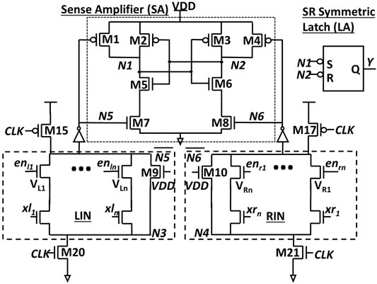
FIGURE 3. Artificial Neuron (AN) Architecture.
3 Neuron Processing Element
The processing element used in this paper is based on the design described in (Wagle et al., 2020). It is used to operate on multi-bit data and is referred to as Neuron Processing Element (NPE) in this paper. The architecture of NPE is shown in Figure 4A. An NPE consists of K (=4) fully connected ANs, denoted by Nk, where k is the index of the neuron. Each AN has a 16-bit local register. The neurons communicate with each other using multiplexers. Each Nk has I (=4) inputs, denoted as xi,k, where i is the index of the input of AN k. The output of AN k at time t is denoted as qk,t. These ANs implement the threshold function [2, 1, 1, 1; T] such that T can take values [1, 2, 3]. The threshold value (T) is assigned during run time using digital control signals. An NPE can perform bitwise logical operations such as (N)AND, (N)OR, NOT, and 3-input majority in a single clock cycle using a single neuron inside it. It is to be noted that, since each neuron in the NPE can process NOT and majority function, CIDAN-XE can support all the functions as described in (Hajinazar et al., 2021) by using majority inverter graph conversion. An NPE can also process 4-bit operands in parallel as it consists of four ANs. Single or multi-bit addition, comparison, pooling, and ReLU operation can be scheduled on the NPE as described in (Wagle et al., 2020). (Wagle et al., 2020) used the NPE to implement binary neural networks (BNNs) with activation and weights being single bit values. In this paper, the NPE is extended to enable multi-bit neural network operations such as multiplication, accumulation, pooling, and various activation functions.
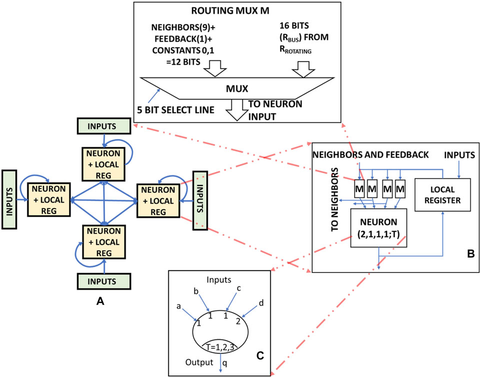
FIGURE 4. (A) Architecture of the Neuron Processing Element (NPE), (B) Artificial neuron (AN) structure and routing infrastructure around it and (C) A single AN used in the NPE.
3.1 Basic Logic Operation on AN
ANs in the NPE implement the threshold function [2, 1, 1, 1; T] which can be reconfigured to perform logic operations on binary operands just by enabling or disabling the required inputs and choosing the appropriate threshold value (T). AN acts as a reconfigurable static gate where the cost of reconfiguration is just the choice of the appropriate inputs and the selection of the threshold value (T). This low reconfiguration cost of the basic elements of the NPE enables the reduction in the overall area and power cost of the processing element. Consider the AN structure as shown in Figure 4C. The binary inputs are a, b, c, and d and the output is y. Table 2 shows the enabled inputs and the threshold values for different bitwise operations on a single AN. 1 bit-addition using XOR and majority operation scheduled on two ANs as shown in the section 3.2.

TABLE 2. Inputs and Threshold selection for various bitwise operation on a single AN. IP1, IP2 and IP3 are input operand bits.
3.2 Multi-Bit Addition and Accumulation Operation
Two m-bit numbers X = xm−1, xm−2, …x1, x0 and Y = ym−1, ym−2, …y1, y0 can be added by mapping a chain of neuron-based ripple carry adders on the NPE. The final sum S = X + Y = {Cm−1, Sm−1, Sm−2, …S1, S0} is generated as follows:
Cycles indexed 0 to m-1 are used to generate the carry bits by mapping the compute of carry function to the third AN of the NPE. Here, the carry function is the majority operation of two input bits xi, yi and the previous carry Ci−1:
Cycles indexed 1 to m are used to generate the sum bits, by mapping the compute of sum function to the second AN of the NPE:
Note that q3,t−1 is supplied to the sum function at time t by using AN 4 as a buffer.
The above mapping is illustrated in Figure 5A. The bits corresponding to X and Y are fetched from the DRAM in one cycle and are stored in the local registers. ANs 1 and 2 then fetch the required bits from the local registers on a cycle-by-cycle basis to do the evaluation. Note that unused inputs of the ANs are connected to 0.
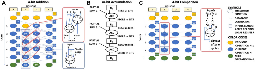
FIGURE 5. (A) 4 bit Addition operation schedule on NPE, (B) m-bit Accumulation operation schedule on NPE and (C) Comparison schedule on NPE.
An accumulation operation of size M is treated as repeated addition of an m-bit number with the accumulated M bit number. NPE supports a maximum of 32-bit accumulation operation. An accumulation schedule on NPE is shown in Figure 5B.
2.3 Multi-Bit Comparison and ReLU
Two m-bit numbers X = xm−1, xm−2, …x1, x0 and Y = ym−1, ym−2, …y1, y0 can be compared (X > Y) in m cycles on the NPE as follows:
The result of X > Y is q1,m. Intuitively, in each cycle, the AN overrides the comparison result that was generated by all the previous lower significance bits if the value of a higher significance bit of X is greater than the value of the respective higher significance bit of Y. As an example, the schedule of 4-bit comparison is shown in Figure 5C.
The ReLU operation, commonly used in neural networks is an extension of the comparison operation. It involves the comparison of an operand against a fixed value. The output of ReLU is the operand itself if it is greater than the fixed value, else the output is 0. This is realized by performing an AND operation of the result of the comparison with the input operand.
3.4 Multi-Bit Multiplication
An NPE acts as a primitive unit for 4-bit multiplication. A multiplication operation is broken into a series bitwise AND and addition operations scheduled on NPE. A schedule of 4-bit multiplication of two operands X = {x3,x2,x1,x0} and Y = {y3,y2,y1,y0} on NPE is shown in the Figure 6A. The multiplication is completed in four steps. Firstly, the partial products P0, P1, P2, P3 are obtained but using four bitwise AND operations on all the ANs in parallel. This step is completed in four cycles. Next, the addition of P0 and 1-bit shifted version of P1 (Sum1) is calculated in 5 clock cycles using the multi-bit addition schedule as shown in the section 3.2. The result Sum1 is stored in the AN N3. Similarly, in the next step addition of P2 and 1-bit shifted version of P3 are added in 5 cycles again with the result (Sum2) stored in the AN N2. In the last step, Sum1 and Sum2 stored in the ANs, N2 and N3 are added in 7 clock cycles as the Sum2 is shifted by 2 bits before addition. The final result of the multiplication (Sum3) is stored in the AN N1. In total, it takes 21 clock cycles to perform a 4-bit multiplication in a single NPE.
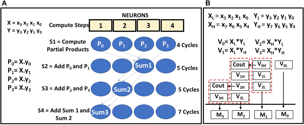
FIGURE 6. (A) 4 bit Multiplication operation schedule on NPE and (B) Multiplication schedule using partial products of decomposed operands. In 4(A) The ANs are labeled with the final result stored in them. Computations however, involve all the four ANs.
For 8 bit operands, the multiplication is broken into smaller multiplication operations that use 4-bit operands, and a final addition schedule is used as shown in Figure 6B. The operands X and Y are decomposed into 4 bit segments as XH, XL, and YH, YL, where the subscripts L and H represent the lower and the upper 4 bits of the 8-bit operand. The partial products of the 4 bit segments is represented as: V0 = XL*YL, V1 = XH*YL, V2 = XL*YH, V3 = XH*YH and executed as 4 bit multiplications on the NPE. After the partial products are obtained, a series of addition operations are carried out as shown in Figure 6B to obtain the final 16 bit result A. For operands of bit width 16 and 32, multiplication can be carried out by recursively breaking up the operands into 4-bit segments and scheduling the operation on the NPE.
3.5 Maxpooling and Average Pooling
The max-pooling operation finds the maximum number in a set defined by the max-pooling window of a neural network. Max-pooling operation is carried out by a series of comparisons, bitwise AND and bitwise OR operation. For illustration, let a max-pooling operation be applied to four n-bit numbers A, B, C, and D. In this case, the pooling window is 2 × 2. The max-pooling operations are illustrated in Figure 7. Bits x, y, and z are binary results of the comparison of different inputs. The result of the max operation after the comparison is obtained using bitwise AND and OR operation of inputs with the comparison result bit as shown the Figure 7. The max-pooling operation involves m-1 comparison operations for a set of m numbers.
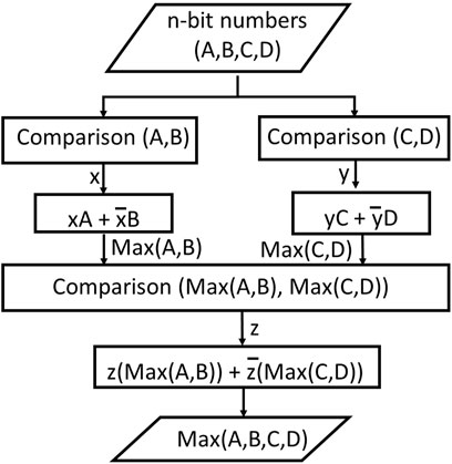
FIGURE 7. Maxpooling operation on pooling window of 2 × 2.
Average pooling is supported for limited pooling windows which have a size in powers of 2, eg., 2 × 2, 4 × 4, 8 × 8, etc. All the numbers in the set are added and then the right shift operation is used to realize division.
4 Top-Level Architecture
Figure 8A shows the logical organization of banks in a DRAM. A group of banks shares the local I/O gating which consists of column multiplexers and write drivers, and therefore only the bank can be accessed for reading or writing by an external compute unit. However, it is possible to activate multiple banks within a group such that the data of a row can be latched to the local bitline sense amplifiers (BLSA). The number of banks that can be simultaneously activated is constrained by the power budget of the DRAM chip. This power constraint is enforced by the timing parameter tFAW, which defines the time frame within which a maximum of four banks can be activated. Hence, within tFAW data from four different banks can be latched into the BLSA and potentially can be used to perform operations. In CIDAN-XE, the NPEs are placed between the BLSA and the local I/O gating to directly connect to the BLSA output as shown in Figure 8B.
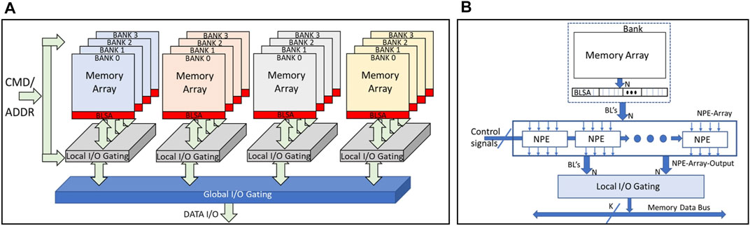
FIGURE 8. (A) DRAM bank organization and (B) Integration of the NPE with a DRAM bank.
An NPE is connected to four BLSA outputs. Hence, if a row buffer has N bits, there are N/4 NPEs connected to the bank. As CIDAN-XE works on four banks in parallel, there are a total of N NPEs in the DRAM. If there are more than four banks in the DRAM, for example, 8 or 16, the NPEs are shared among all the banks using multiplexers but the number of NPEs stays constant to utilize only four banks in parallel. An NPE-array works on the operands derived from the same bank using sequential row activation commands. All the NPEs perform the same operation and share the control signals generated by an external controller. Once the operands are obtained in the NPEs, all the active banks can be precharged together. The latency of precharging the banks is overlapped with the compute latency of NPEs. An NPE can write the results back to the same bank by driving all the bitlines connected to it through BLSA. To write data to another bank, a local shared buffer among different banks is used. Writing an entire row-wide data to another bank is a slower operation than writing back to the bank itself because of the limited capacity of the shared buffer. There are eight rows reserved per bank to write the output data generated from the NPE-array.
4.1 System Level Integration of CIDAN-XE
CIDAN-XE is used as a memory and as an external accelerator that is interfaced with the CPU. The design of CIDAN-XE includes the addition of some special instructions to the CPU’s instruction set that specifies the data and the operation to be carried out in the CIDAN-XE. There are unused opcodes in the CPU instruction set which can be re-purposed to define the instructions for CIDAN-XE. A block diagram representing system-level integration of CIDAN-XE is shown in Figure 9A. An application is modified to include the CIDAN-XE instructions to replace the code which can be executed on the CIDAN-XE platform in parallel. Whenever the CPU identifies CIDAN-XE-specific instruction in the application, it passes it to the CIDAN-XE controller—a state machine that decodes the instruction and generates DRAM commands and control signals to implement the specified operation by the instruction on CIDAN-XE. Extra bits are added to the CPU-memory bus to accommodate the control signals from the CIDAN-XE controller.
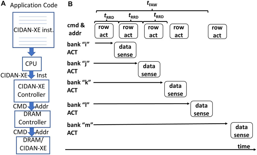
FIGURE 9. (A) System-level Integration of DRAM and (B) Activation commands to different banks within four bank activation window.
CIDAN-XE tries to utilize a maximum of four banks in parallel, therefore, the operands are pre-arranged across the banks for a row address before moving on to the next row. For every operation, to transfer the operand to the NPEs, the activation command for a row is generated sequentially separated by tRRD time. The operand data is latched to local registers of the NPE from the BLSA. The activation commands are followed by a single precharge command which precharges all the active banks. The same set of commands is issued to get more operands or more bits of the operands if the operand bit width is greater than four. After the operands are obtained, the NPE operates and then writes back the data to the reserved rows for the output in the same bank itself or to another bank using the shared internal buffer. An operation sequence on a single bank of DRAM to obtain two operands to the connected NPE, perform an operation, and write back the result is shown in the Eq. 6. The compute on NPE is selected using the control signals from the CIDAN-XE controller. It should be noted that in the operation of CIDAN-XE, no existing protocol or timing constraints of the DRAM are violated even when operating multiple banks in parallel. Therefore, no changes to the row decoder or memory controller are required to facilitate complex DRAM operations as done in the prior work (Li et al., 2017; Seshadri et al., 2017; Deng et al., 2018; Hajinazar et al., 2021).
5 Case Study: Convolution Neural Networks Inference
In this section, we take convolutional neural network inference to exemplify the use of the CIDAN-XE platform for varying bit-precision workloads and obtaining high throughput and energy efficiency. We show the data mapping for CNN applications to achieve maximum throughput. It should be, however, noted that CIDAN-XE platform is not limited to the inference of CNNs.
The accuracy of CNN inference tasks varies with the bit-precision (McKinstry et al., 2019; Sun et al., 2020). The accuracy is highest for floating-point representation and decreases as the bit precision is lowered to a fixed-point representation of 8, 4, 2 bits, and in the extreme case to 1 bit. The CNN with 1-bit precision of inputs and weights are called Binary Neural Networks (BNN) (Courbariaux and Bengio, 2016) and the networks with only weights being restricted to binary values are called Binary Weighted Networks (BWNs) (Courbariaux et al., 2015). In BWNs the inputs may have bit-precision of 4-bits, 8-bits, or 16-bits. The lower precision networks substantially reduce the memory requirements and computational load for the hardware implementation and are suitable for a resource-constrained implementation. Hence, there exists a trade-off between the accuracy and the available hardware resources while selecting the bit-precision of CNNs. It will be shown in Section 6 that CIDAN-XE implements various fixed precision networks, achieving a higher throughput and energy efficiency over the prior work.
5.1 Data Mapping of CNNs Onto DRAM
A CNN mostly consists of three types of layers: the convolution layer, the pooling layer, and the fully connected layer. A convolution layer operation is depicted in the Figure 10A. In this operation, an input of dimension I*I*C is convolved with different kernels of size K*K*C to produce an output feature map of size F*F. If there are M kernels, M output feature maps are produced.
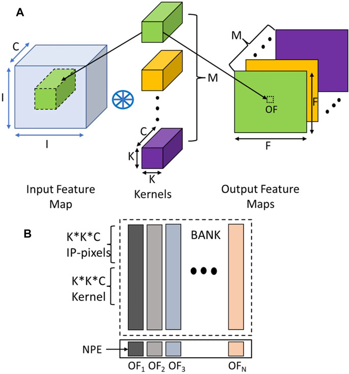
FIGURE 10. (A) Convolution Operations with its important parameters and (B) Data mapping into DRAM banks for the Convolution layer.
To compute one output feature (OF) a K*K*C kernel is convolved with a section of the image of the same dimensions. As all the NPEs are connected to different bitlines, they can work independently on the data residing in different rows connected to the same set of bitlines. Hence, each NPE can produce one output feature. Since all NPEs work in parallel, they can be fully utilized to produce several output features in parallel in the same number of cycles for a given layer. Therefore, the required input and kernel pixels are arranged vertically in the columns connected to an NPE. The input pixels and kernel pixels are replicated along the columns of a bank to support the parallel operation of all the NPEs to generate output feature maps. Figure 10B shows data mapping along with vertical columns in banks, where columns act as a Single Instruction Multiple Data (SIMD) lane connected to an NPE.
The pooling and the fully connected layers can be converted to the convolution layer using the parameters I, C, K, F, M. The input is mapped to DRAM banks such that an output value can be produced by a single PE over multiple cycles and the maximum NPEs can be used in parallel. A data mapping algorithm is designed to achieve mapping to use the maximum number of NPEs in parallel and achieve the maximum possible throughput. The data mapping algorithm tries to avoid any movement of data from one NPE to another in a single bank as shifting of data through shared internal buffer using CPU instructions is expensive in terms of latency and energy.
6 Experimental Results
6.1 Evaluation of Processing in DRAM Architectures
Most PIM architectures include modification to the DRAM address decoding circuits, analog operation of the memory array, or the addition of extra logic circuits to the DRAM. To evaluate such changes, first, the circuit level simulations and characterization of the building blocks of extensions/modifications to DRAM using SPICE-like tools are carried out. Using the circuit level characterization data, industry-standard synthesis tools are used to design and evaluate the entire DRAM modifications. These evaluations are carried out at logic process technology whereas, the changes are proposed in the DRAM technology. Hence, the area and performance numbers from the synthesis tools are scaled to DRAM technology using some prior established scaling factors. To simulate the entire PIM architecture using an application, a behavioral-level simulator is designed either independently or with existing DRAM simulators to calculate energy and latency.
The proposed design CIDAN-XE follows the same established evaluation methodology. The AN is designed in TSMC 40 nm LP process technology. It was rigorously tested for functional correctness and for robustness against process variations using Monte-Carlo simulations in HSPICE (Wagle et al., 2019). The neural processing elements (NPEs) are synthesized, placed, and routed using Cadence Genus and Innovus tools. We used the standard cell library of TSMC 40 nm LP technology and an in-house characterized standard cell library of the AN. The area, power, and energy numbers are extracted from the design tools and scaled to the DRAM technology using the previous research work (Yong-Bin and Chen, 1996). A behavioral level simulator is developed in concert with an existing DRAM energy simulator called DRAMPower (Chandrasekar et al., 2021) to simulate the overall latency and the energy of various workloads on the PIM platform. The workload description and the memory specification are provided to this simulator as input.
6.2 Raw Performance and Energy Analysis
The proposed PIM platform CIDAN-XE can perform more basic operations than the ones explained in the section 3. In this section for raw throughput and energy analysis, we implement fifteen basic operations. These operations chosen for evaluation consists of a mix of functions from bitwise logic operations to multiplication operation. The evaluation is done using a synthetic workload with an operand size of 64 million elements with each element size of 32 bits using the behavioral level simulator. The memory specifications of the DDR4-2400 memory with the row buffer size of 8 KB are used for the simulation.
CIDAN-XE is evaluated against a CPU (Intel Skylake, 16 cores, 4 GHz), GPU (NVIDIA Titan V, 5120 CUDA cores, 1.2 GHz) and some prior PIM architectures such as AMBIT:1B and SIMDRAM:4B using the data from (Hajinazar et al., 2021). Note, all the PIM architectures are evaluated on the same memory specifications.
In SIMDRAM:4B, four banks are operated in parallel and AMBIT:1B operates on a single bank. CIDAN-XE:4B operates on four banks in parallel under the tFAW timing constraint. Therefore, SIMDRAM:4B and CIDAN-XE:4B have equal parallelism in their designs.
Figure 11A shows raw throughput comparison of CIDAN-XE with the state-of-the-art PIM architectures, CPU, and GPU. SIMDRAM:4B and CIDAN-XE:4B use four banks in parallel and hence are equivalent designs for a comparison. CIDAN-XE:4B on average over the fifteen reported functions has 6.3X higher throughput than SIMDRAM:4B. Against the CPU/GPU, CIDAN-XE:4B has a throughput improvement of the order of 72X/5.4X. To understand the reason for the higher throughput that CIDAN-XE:4B achieves than AMBIT:1B, and SIMDRAM:4B, it is necessary to look into the basic operation of these architectures.
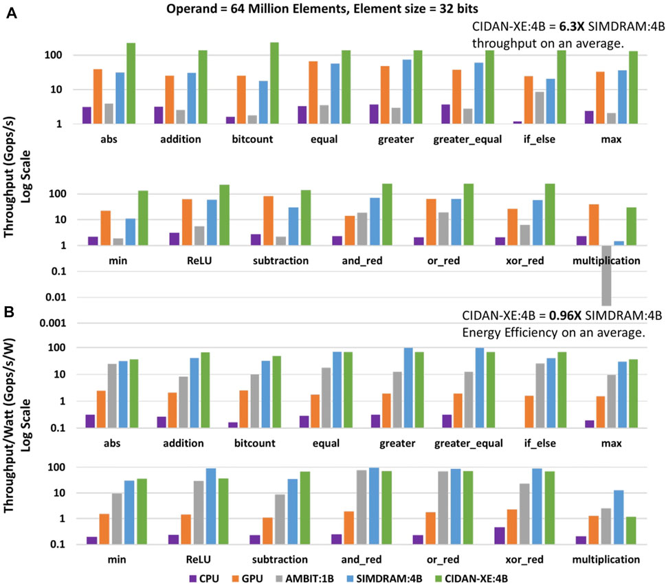
FIGURE 11. Throughput (A) and Energy Efficiency (B) comparison of CIDAN-XE with CPU, GPU and other PIM architectures.
In the section 2.3, the majority function computation on three rows in AMBIT is shown. The majority operation is carried out using multi-cycle AAP/AP DRAM command primitives. In SIMDRAM, a framework is developed to convert any desired operation into an optimized majority/not implementation. Thereafter, a micro-program is developed by converting the majority/not graph to AAP/AP primitives for final execution onto the DRAM. For example, a 1-bit addition on SIMDRAM requires 7 AAP and 2 AP operations which takes hundreds of cycles. On the other hand, a 1-bit addition operation in CIDAN-XE:4B requires only to activate two rows followed by precharge to get the operands, and only 2 cycles on NPE to perform 1-bit addition.
Figure 11B shows the energy efficiency of the CIDAN-XE:4B over the baseline CPU for the fifteen basic operations. CIDAN-XE:4B achieves about 244X higher energy efficiency than CPU. The SIMDRAM:4B design report about 257X higher energy efficiency as compared to the baseline CPU. SIMDRAM achieves high energy efficiency because of the involvement of only memory rows for computation rather than having external gates for computing. The CIDAN-XE manages to match the energy efficiency of the SIMDRAM design despite having external NPE for computing. CIDAN-XE requires a very small number of compute cycles on NPE as compared to the total memory cycles for computation in SIMDRAM, which reduces the proportion of NPE in the total energy of CIDAN-XE and enables high energy efficiency. With equivalent energy efficiency and much higher throughput, CIDAN-XE is a more efficient PIM platform as compared to the state-of-the-art PIM architecture SIMDRAM.
6.3 CNN Case Study Analysis
CIDAN-XE is evaluated over five different neural networks: ALEXNET (Krizhevsky et al., 2012), RESNET-18, RESNET-50 (He et al., 2015), VGG-16, VGG-19 (Simonyan and Zisserman, 2015) for various bit-precision of inputs and weights. The input to the network is an image of size 224 × 224 × 3 and the DRAM used is DDR4-2400 with 4 Gb of capacity. The DRAM has 1 channel, 1 rank, 16 banks, with a row buffer of size 8 Kbits. CIDAN-XE uses 8192 NPEs for the CNN inference implementation.
6.3.1 Throughput and Energy Efficiency Analysis
The different evaluation modes based on the bit-precision of the inputs and weights used in the CNNs implementation on CIDAN-XE are shown in Table 3. Figure 12A shows the throughput (Frames/s) by using a batch size of 1 on the CIDAN-XE platform for different CNNs in all the evaluation modes. The latency incurred for any operation on CIDAN-XE can be divided into two parts: the latency of operands delivery to NPE from the memory banks and the latency of computation on the NPE itself. It is observed that the 8-bit mode has the lowest throughput among all the evaluation modes and the 4-bit mode has the highest throughput. This is because of two reasons based on the analysis of the two latency components. First, the operands are decomposed into 4 bits segments and stored in consecutive rows sharing the same columns and the NPE. Hence, it requires multiple sequential row activations on the same bank to read operands into the NPE. Second, the NPE is designed as a 4-bit compute primitive, hence, the computation for 4-bit mode is optimized which leads to high throughput. The computation latency for the binary-weighted (BW) networks is also low as the costly multiplication operation is reduced to AND operation and the other operations are also simplified. Hence, the throughput is high for binary-weighted (BW) evaluation modes as well.
TABLE 3. Evaluation modes description of Neural Networks.
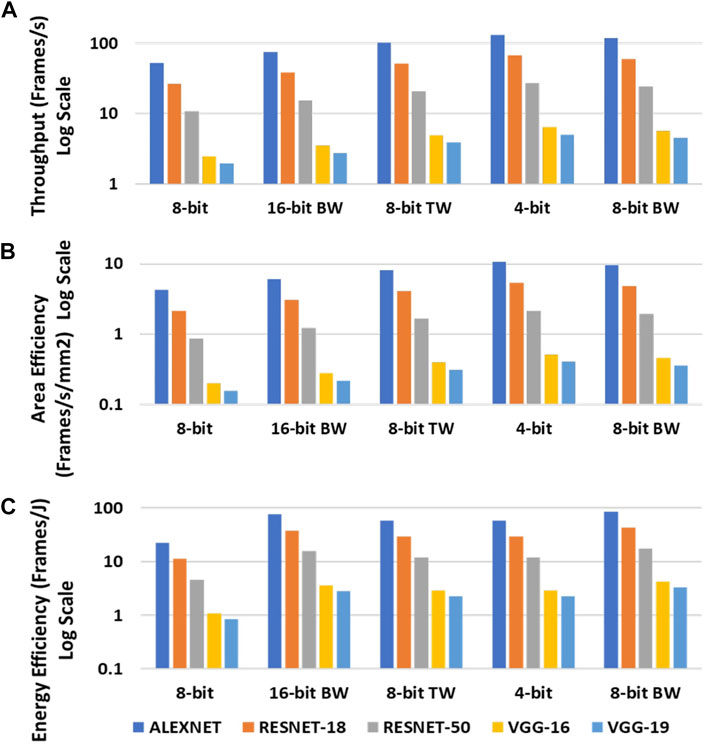
FIGURE 12. Throughput (A), Area-efficiency (B) and Energy efficiency (C) for CIDAN-XE, for CNN networks of varying bit-precision.
The throughput is also proportional to the computational load of the neural networks. ALEXNET with the least number of operations has the highest throughput among all the evaluation modes and the VGG-19 has the least throughput on account of having the most number of operations. The throughput normalized by area representing the area efficiency is shown in Figure 12B.
The energy efficiency represented as the Frames/joule or the Throughput/Watt in the CNN inference application is dominated by the energy of computation on the NPEs rather than the energy consumption of the delivery of the operands to the NPE. This is because the complex operations carried out on the NPE for CNN’s takes multiple cycles and consequently consume more energy. Hence, it is observed that the binary-weighted evaluation mode has the highest energy efficiency and the 8-bit mode has the lowest energy efficiency. Figure 12C shows the energy efficiency of CIDAN-XE for all evaluation modes for different neural networks.
6.3.2 Comparison With Other Architectures
In this section, a comparison of CIDAN-XE with other hardware platforms and prior PIM architectures is discussed. The CNN workload chosen for comparison is ALEXNET. The compared designs include the state-of-the-art Von-Neumann machines such as Intel Knights Landing (KNL) CPU Sodani, 2015) and Nvidia Tesla P100 GPU (Awan et al., 2017); industry-standard CNN accelerators such as Google Tensor Processing Unit (TPU) (Sutradhar et al., 2022) and Intel Movidius Neural Compute Stick (NCS) (Sutradhar et al., 2022); internal processing in memory (iPIM) architectures such as Neural Cache, DRISA, DrACC, and a LUT-based design Lacc. Neural Cache is based on SRAM cache modifications, DRISA and DrAcc are based on logic operations using memory arrays and custom logic, and Lacc is an LUT-based PIM implemented on the DRAM platform. It should be noted that all the prior PIM architectures are implemented using 28 nm or lower process technology and CIDAN-XE is implemented in 40 nm technology node. The results show CIDAN-XE’s improvements over the prior PIM and other architectures without scaling and the improvements are bound to increase if the performance and energy efficiency of CIDAN-XE is scaled to 28 nm or lower technology node.
Figure 13A shows the throughput and Figure 13B shows the energy efficiency of CIDAN-XE in different evaluation modes versus the other architectures using the ALEXNET workload with an input image size of 224 × 224 × 3. DRISA has the highest throughput using the binary-weighted (BW) implementation of ALEXNET. CIDAN-XE in the 8-bit BW mode has a comparable throughput to DRISA with a 5.6X higher energy efficiency. DrAcc operating in 8 bit ternary weight (TW) mode has the highest energy efficiency among the prior PIM architectures which is comparable to CIDAN-XE 8-bit TW mode. CIDAN-XE 8 bit TW has about 1.2X higher throughput when DrAcc is operated in its high throughput configuration. In this configuration, the latency of DrAcc is 386.4 s, whereas, the latency of CIDAN-XE 8 bit TW is 9.7 ms which is three orders of magnitude less than the DrAcc. In high-speed mode, DrAcc has a latency of 275 ms which is still 28X more than the CIDAN-XE 8 bit TW while the DrAcc’s throughput drops to 3.63 Frames/s. CIDAN-XE 8 bit TW has a throughput of 102 Frames/s. Hence, CIDAN-XE is a high throughput and highly energy-efficient architecture and shows considerable improvements over the prior PIM architectures.
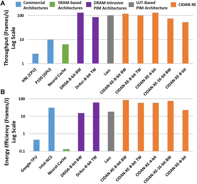
FIGURE 13. Throughput (A) and energy-efficiency (B) comparison of CIDAN-XE against the state of the art architectures when computing ALEXNET.
6.3.3 Cost Analysis
An NPE consists of ANs in the form of standard cells (Wagle et al., 2019) and some other standard cells from the TSMC 40 nm LP library. The physical layout of the ANs uses only two metal layers and all the other standard cells have a single metal layer. Hence, the NPE is completely DRAM process technology compatible which allows 3-4 metal layers in the design. The area of each NPE is 1536 µm2. There are a total of 8192 NPEs used in the DDR4-2400 memory with a row buffer size of 8 Kbits and a total capacity of 4 Gbits. The total area overhead the design is 12.6 mm2at 40 nm technology node.
7 Conclusion
In this paper, we presented a novel artificial neuron-based PIM architecture on a DRAM platform. Each processing element, called neuron processing element (NPE), used in this architecture, can perform arithmetic, logical, relational, and a few other complex operations such as comparison, ReLU, etc. We presented the inference task in the CNNs as a case study to showcase the potential of the CIDAN-XE to execute complex operations at various bit precision of its inputs. CIDAN-XE improves upon the latest Von-Neumann designs, industry-standard CNN accelerators, and other PIM architectures in the throughput and energy efficiency for an equivalent workload. Although only the CNN application is demonstrated, the CIDAN-XE platform is amenable to many other data-intensive applications given the diversity of the operations that CIDAN-XE can perform as shown in this paper. Improvements demonstrated in this paper are attributed to the combined benefits that come from using the local storage present in the NPE, alongside the ability of the NPEs to be reconfigured to implement various functions with very low reconfiguration cost. CIDAN-XE platform in particular is suitable for application that operates on large input vectors and matrices such as encryption, graph analysis, bioinformatics, etc.
Data Availability Statement
The original contributions presented in the study are included in the article/Supplementary Material, further inquiries can be directed to the corresponding author.
Author Contributions
All authors listed have made a substantial, direct, and intellectual contribution to the work and approved it for publication.
Funding
This research was supported in part by NSF Grant #2008244, and by the Center for Embedded Systems, NSF Grant #1361926.
Conflict of Interest
The authors declare that the research was conducted in the absence of any commercial or financial relationships that could be construed as a potential conflict of interest.
Publisher’s Note
All claims expressed in this article are solely those of the authors and do not necessarily represent those of their affiliated organizations, or those of the publisher, the editors, and the reviewers. Any product that may be evaluated in this article, or claim that may be made by its manufacturer, is not guaranteed or endorsed by the publisher.
Footnotes
1W.L.O.G. the weights wi and threshold T can be integers (Muroga, 1971).
References
Ali, M. F., Jaiswal, A., and Roy, K. (2020). In-memory Low-Cost Bit-Serial Addition Using Commodity Dram Technology. IEEE Trans. Circuits Syst. I 67 (1), 155–165. doi:10.1109/tcsi.2019.2945617
Angizi, S., and Fan, D. (2019). “GraphiDe: A Graph Processing Accelerator Leveraging In-DRAM-Computing,” in GLSVLSI ’19: Great Lakes Symposium on VLSI 2019, Tysons Corner, VA, United States, May 9–11, 2019, 45–50.
Angizi, S., and Fan, D. (2019). “ReDRAM: A Reconfigurable Processing-In-DRAM Platform for Accelerating Bulk Bit-Wise Operations,” in 2019 IEEE/ACM International Conference on Computer-Aided Design (ICCAD), Westminster, CO, United States, November 4–7, 2019, 1–8. doi:10.1109/iccad45719.2019.8942101
Angizi, S., He, Z., Reis, D., Hu, X. S., Tsai, W., Lin, S. J., et al. (2019). “Accelerating Deep Neural Networks in Processing-In-Memory Platforms: Analog or Digital Approach,” in 2019 IEEE Computer Society Annual Symposium on VLSI (ISVLSI), Miami, FL, United States, July 15–17, 2019, 197–202.
Awan, A. A., Subramoni, H., and Panda, D. K. (2017). “An In-Depth Performance Characterization of Cpu- and Gpu-Based Dnn Training on Modern Architectures,” in Proceedings of the Machine Learning on HPC Environments, Denver, CO, United States, November 12–17, 2017 (ACM), 1–8. doi:10.1145/3146347.3146356
Boroumand, A., Ghose, S., Kim, Y., Ausavarungnirun, R., Shiu, E., Thakur, R., et al. (2018). Google Workloads for Consumer Devices. SIGPLAN Not. 53 (2), 316–331. doi:10.1145/3296957.3173177
Chandrasekar, K., Weis, C., Li, Y., Goossens, S., Jung, M., Naji, O., et al. (2021). DRAMPower: Open-Source DRAM Power and Energy Estimation Tool. Available at: http://www.drampower.info/. (Accessed May 16, 2021).
Chi, P., Li, S., Xu, C., Zhang, T., Zhao, J., Liu, Y., et al. (2016). Prime: a Novel Processing-In-Memory Architecture for Neural Network Computation in Reram-Based Main Memory. SIGARCH Comput. Archit. News 44 (3), 27–39. doi:10.1145/3007787.3001140
Courbariaux, M., and Bengio, Y. (2016). Binarynet: Training Deep Neural Networks with Weights and Activations Constrained to +1 or -1. CoRR, abs/1602.02830.
Courbariaux, M., Bengio, Y., and David, J. (2015). “Binaryconnect: Training Deep Neural Networks with Binary Weights during Propagations,” in Advances in Neural Information Processing Systems (Montreal, Canada: MIT Press), 3123–3131.
Dai, Z., Liu, H., Le, Q. V., and Tan, M. (2021). Coatnet: Marrying Convolution and Attention for All Data Sizes. arXiv.
Dally, B. (2015). Challenge for Future Computer Systems. Available at: https://www.cs.colostate.edu/ cs575dl/Sp2015/Lectures/Dally2015.pdf. (Accessed December 7, 2021).
Deng, Q., Jiang, L., Zhang, Y., Zhang, M., and Yang, J. (2018). “DrAcc: a DRAM Based Accelerator for Accurate CNN Inference,” in 2018 55th ACM/ESDA/IEEE Design Automation Conference (DAC), San Francisco, CA, United States, June 24–28, 2018, 1–6. doi:10.1109/dac.2018.8465866
Deng, Q., Zhang, Y., Zhang, M., and Yang, J. (2019). “Lacc: Exploiting Lookup Table-Based Fast and Accurate Vector Multiplication in Dram-Based Cnn Accelerator,” in 2019 56th ACM/IEEE Design Automation Conference (DAC), Las Vegas, NV, United States, June 2–6, 2019, 1–6.
Ferreira, J. D., Falcão, G., Luna, J. G., Alser, M., Orosa, L., Sadrosadati, M., et al. (2021). Pluto: In-Dram Lookup Tables to Enable Massively Parallel General-Purpose Computation. CoRR, abs/2104.07699.
Gokhale, M., Cohen, J., Yoo, A., Miller, W. M., Jacob, A., Ulmer, C., et al. (2008). Hardware Technologies for High-Performance Data-Intensive Computing. Computer 41 (4), 60–68. doi:10.1109/mc.2008.125
Guo, X., Merrikh Bayat, F., Bavandpour, M., Klachko, M., Mahmoodi, M. R., Prezioso, M., et al. (2017). “Fast, Energy-Efficient, Robust, and Reproducible Mixed-Signal Neuromorphic Classifier Based on Embedded NOR Flash Memory Technology,” in 2017 IEEE International Electron Devices Meeting (IEDM), San Francisco, CA, United States, December 2–6, 2017, 6.5.1–6.5.4. doi:10.1109/iedm.2017.8268341
Hajinazar, N., Oliveira, G. F., Gregorio, S., Ferreira, J. D., Ghiasi, N. M., Patel, M., et al. (2021). “SIMDRAM: a Framework for Bit-Serial SIMD Processing Using DRAM,” in ASPLOS ’21: 26th ACM International Conference on Architectural Support for Programming Languages and Operating Systems, April 19–23, 2021, 329–345. doi:10.1145/3445814.3446749
He, K., Zhang, X., Ren, S., and Sun, J. (2015). Deep Residual Learning for Image Recognition. CoRR, abs/1512.03385.
He, M., Song, C., Kim, I., Jeong, C., Kim, S., Park, I., et al. (2020). “Newton: A DRAM-Maker’s Accelerator-In-Memory (AiM) Architecture for Machine Learning,” in 2020 53rd Annual IEEE/ACM International Symposium on Microarchitecture (MICRO), Athens, Greece, October 17–21, 2020, 372–385.
Huangfu, W., Li, X., Li, S., Hu, X., Gu, P., and Xie, Y. (2019). “Medal: Scalable Dimm Based Near Data Processing Accelerator for Dna Seeding Algorithm,” in Proceedings of the 52nd Annual IEEE/ACM International Symposium on Microarchitecture, MICRO ’52, New York, NY, United States, October 12–16, 2019 (Association for Computing Machinery), 587–599.
Jacob, B., Ng, S. W., and Wang, D. T. (2008). Memory Systems: Cache, DRAM, Disk. Boston, United States: Morgan Kaufmann Publishers.
Judd, P., Albericio, J., Hetherington, T., Aamodt, T. M., and Moshovos, A. (2016). “Stripes: Bit-Serial Deep Neural Network Computing,” in 2016 49th Annual IEEE/ACM International Symposium on Microarchitecture (MICRO), Taipei, Taiwan, October 15–19, 2016 (IEEE), 1–12. doi:10.1109/micro.2016.7783722
Krizhevsky, A., Sutskever, I., and Hinton, G. E. (2012). “Imagenet Classification with Deep Convolutional Neural Networks,” in Proceedings of the 25th International Conference on Neural Information Processing Systems-NIPS’12, Lake Tahoe, NV, United States, December 3–6, 2012 (Red Hook, NY, USA: Curran Associates Inc), 1097–1105.
Kulkarni, N., Yang, J., Seo, J.-S., and Vrudhula, S. (2016). Reducing Power, Leakage, and Area of Standard-Cell ASICs Using Threshold Logic Flip-Flops. IEEE Trans. VLSI Syst. 24 (9), 2873–2886. doi:10.1109/tvlsi.2016.2527783
Kwon, Y., Lee, S. H., Lee, J., Kwon, S., Ryu, J. M., Son, J., et al. (2021). “25.4 A 20nm 6GB Function-In-Memory DRAM, Based on HBM2 with a 1.2TFLOPS Programmable Computing Unit Using Bank-Level Parallelism, for Machine Learning Applications,” in 2021 IEEE International Solid- State Circuits Conference (ISSCC), San Francisco, CA, United States, February 13–22, 2021, 350–352. doi:10.1109/isscc42613.2021.9365862
Li, D., Chen, X., Becchi, M., and Zong, Z. (2016). “Evaluating the Energy Efficiency of Deep Convolutional Neural Networks on Cpus and Gpus,” in 2016 IEEE International Conferences on Big Data and Cloud Computing (BDCloud), Social Computing and Networking (SocialCom), Sustainable Computing and Communications (SustainCom) (BDCloud-SocialCom-SustainCom), Atlanta, GA, United States, October 8–10, 2016, 477–484. doi:10.1109/bdcloud-socialcom-sustaincom.2016.76
Li, S., Niu, D., Malladi, K. T., Zheng, H., Brennan, B., and Xie, Y. (2017). “DRISA: a DRAM-Based Reconfigurable In-Situ Accelerator,” in Proceedings of the 50th Annual IEEE/ACM International Symposium on Microarchitecture, Boston, MA, United States, October 14–17, 2017, 288–301.
McKinstry, J. L., Esser, S. K., Appuswamy, R., Bablani, D., Arthur, J. V., Yildiz, I. B., et al. (2019). “Discovering Low-Precision Networks Close to Full-Precision Networks for Efficient Inference,” in 2019 Fifth Workshop on Energy Efficient Machine Learning and Cognitive Computing - NeurIPS Edition (EMC2-NIPS), Vancouver, BC, Canada, December 13, 2019, 6–9. doi:10.1109/emc2-nips53020.2019.00009
Muroga, S. (1971). Threshold Logic and its Applications. New York, United States: Wiley-Interscience.
Myers, G. (1999). A Fast Bit-Vector Algorithm for Approximate String Matching Based on Dynamic Programming. J. ACM 46 (3), 395–415. doi:10.1145/316542.316550
Seshadri, V., Kozuch, M. A., Mowry, T. C., Kim, Y., Fallin, C., Lee, D., et al. (2013). “RowClone: Fast and Energy-Efficient In-DRAM Bulk Data Copy and Initialization,” in Proceedings of the 46th Annual IEEE/ACM International Symposium on Microarchitecture - MICRO-46, Davis, CA, United States, December 7–11, 2019, 185–197.
Seshadri, V., Lee, D., Mullins, T., Hassan, H., Boroumand, A., Kim, J., et al. (2017). “Ambit: In-Memory Accelerator for Bulk Bitwise Operations Using Commodity DRAM Technology,” in Proceedings of the 50th Annual IEEE/ACM International Symposium on Microarchitecture, Boston, MA, United States, October 14–17, 2017, 273–287.
Simonyan, S., and Zisserman, A. (2015). Very Deep Convolutional Networks for Large-Scale Image Recognition. CoRR, abs/1409.1556
Singh, G., Wagle, A., Vrudhula, S., and Khatri, S. (2021). “Cidan: Computing in Dram with Artificial Neurons,” in 2021 IEEE 39th International Conference on Computer Design (ICCD), Storrs, CT, United States, Storrs 24–27, 2021, 349–356. doi:10.1109/iccd53106.2021.00062
Sodani, A. (2015). “Knights landing (Knl): 2nd Generation Intel® Xeon Phi Processor,” in 2015 IEEE Hot Chips 27 Symposium (HCS), Cupertino, CA, United States, August 22–25, 2015 (IEEE), 1–24.
Sun, X., Wang, N., Chen, C., Ni, J., Agrawal, A., Cui, X., et al. (2020). “Ultra-low Precision 4-bit Training of Deep Neural Networks,” in Advances in Neural Information Processing Systems (Vancouver, Canada: Curran Associates, Inc.), Vol. 33, 1796–1807.
Sutradhar, P. R., Bavikadi, S., Connolly, M., Prajapati, S., Indovina, M. A., Dinakarrao, S. M. P., et al. (2022). Look-up-table Based Processing-In-Memory Architecture with Programmable Precision-Scaling for Deep Learning Applications. IEEE Trans. Parallel Distrib. Syst. 33 (2), 263–275. doi:10.1109/tpds.2021.3066909
Vrudhula, S., Kulkami, N., and Yang, J. (2015). “Design of Threshold Logic gates Using Emerging Devices,” in 2015 IEEE International Symposium on Circuits and Systems (ISCAS), Lisbon, Portugal, May 24–27, 2015 (IEEE), 373–376. doi:10.1109/iscas.2015.7168648
Wagle, A., Singh, G., Yang, J., Khatri, S., and Vrudhula, S. (2019). “Threshold Logic in a Flash,” in 2019 IEEE 37th International Conference on Computer Design (ICCD), Abu Dhabi, United Arab Emirates, November 17–20, 2019, 550–558. doi:10.1109/iccd46524.2019.00081
Wagle, A., Khatri, S., and Vrudhula, S. (2020). “A Configurable BNN ASIC Using a Network of Programmable Threshold Logic Standard Cells,” in 2020 IEEE 38th International Conference on Computer Design (ICCD), Hartford, CT, United States, October 18–21, 2020 (IEEE), 433–440. doi:10.1109/iccd50377.2020.00079
Xin, X., Zhang, Y., and Yang, J. (2020). “Elp2im: Efficient and low power bitwise operation processing in dram,” in 2020 IEEE International Symposium on High Performance Computer Architecture (HPCA), San Diego, CA, United States, February 22–26, 2020 (IEEE), 303–314. doi:10.1109/hpca47549.2020.00033
Yang, J., Kulkarni, N., Yu, S., and Vrudhula, S. (2014). “Integration of Threshold Logic gates with RRAM Devices for Energy Efficient and Robust Operation,” in 2014 IEEE/ACM International Symposium on Nanoscale Architectures (NANOARCH), Paris, France, July 8–10, 2014 (IEEE), 39–44. doi:10.1109/nanoarch.2014.6880500
Yang, J., Davis, J., Kulkarni, N., Seo, J., and Vrudhula, S. (2015). “Dynamic and Leakage Power Reduction of ASICs Using Configurable Threshold Logic gates,” in 2015 IEEE Custom Integrated Circuits Conference (CICC), San Jose, CA, United States, September 28–30, 2015 (IEEE), 1–4. doi:10.1109/cicc.2015.7338369
Yin, S., Jiang, Z., Kim, M., Gupta, T., Seok, M., and Seo, J.-S. (2020). Vesti: Energy-Efficient In-Memory Computing Accelerator for Deep Neural Networks. IEEE Trans. VLSI Syst. 28 (1), 48–61. doi:10.1109/tvlsi.2019.2940649
Keywords: artificial neuron, processing in-memory, in-memory computing, DRAM, memory wall, energy efficient architectures, data-intensive applications
Citation: Singh G, Wagle A, Khatri S and Vrudhula S (2022) CIDAN-XE: Computing in DRAM with Artificial Neurons. Front. Electron. 3:834146. doi: 10.3389/felec.2022.834146
Received: 13 December 2021; Accepted: 24 January 2022;
Published: 18 February 2022.
Edited by:
Ram Krishnamurthy, Intel, United StatesReviewed by:
Jae-sun Seo, Arizona State University, United StatesXueqing Li, Tsinghua University, China
Copyright © 2022 Singh, Wagle, Khatri and Vrudhula. This is an open-access article distributed under the terms of the Creative Commons Attribution License (CC BY). The use, distribution or reproduction in other forums is permitted, provided the original author(s) and the copyright owner(s) are credited and that the original publication in this journal is cited, in accordance with accepted academic practice. No use, distribution or reproduction is permitted which does not comply with these terms.
*Correspondence: Sarma Vrudhula, vrudhula@asu.edu