All-in-Memory Brain-Inspired Computing Using FeFET Synapses
 Simon Thomann
  Hong L. G. Nguyen
 Paul R. Genssler
 Hussam Amrouch
- Chair of Semiconductor Test and Reliability (STAR), University of Stuttgart, Stuttgart, Germany
The separation of computing units and memory in the computer architecture mandates energy-intensive data transfers creating the von Neumann bottleneck. This bottleneck is exposed at the application level by the steady growth of IoT and data-centric deep learning algorithms demanding extraordinary throughput. On the hardware level, analog Processing-in-Memory (PiM) schemes are used to build platforms that eliminate the compute-memory gap to overcome the von Neumann bottleneck. PiM can be efficiently implemented with ferroelectric transistors (FeFET), an emerging non-volatile memory technology. However, PiM and FeFET are heavily impacted by process variation, especially in sub 14 nm technology nodes, reducing the reliability and thus inducing errors. Brain-inspired Hyperdimensional Computing (HDC) is robust against such errors. Further, it is able to learn from very little data cutting energy-intensive transfers. Hence, HDC, in combination with PiM, tackles the von Neumann bottleneck at both levels. Nevertheless, the analog nature of PiM schemes necessitates the conversion of results to digital, which is often not considered. Yet, the conversion introduces large overheads and diminishes the PiM efficiency. In this paper, we propose an all-in-memory scheme performing computation and conversion at once, utilizing programmable FeFET synapses to build the comparator used for the conversion. Our experimental setup is first calibrated against Intel 14 nm FinFET technology for both transistor electrical characteristics and variability. Then, a physics-based model of ferroelectric is included to realize the Fe-FinFETs. Using this setup, we analyze the circuit’s susceptibility to process variation, derive a comprehensive error probability model, and inject it into the inference algorithm of HDC. The robustness of HDC against noise and errors is able to withstand the high error probabilities with a loss of merely 0.3% inference accuracy.
1 Introduction
The recent trend towards data-centric applications, like deep neural networks and big data analysis, challenges the current computer architectures. The large energy cost of data transfers renders the von Neumann architecture inefficient for such data-centric workloads. A result of this separation between compute and memory units is the “memory wall”. To tackle this problem effectively, advances across the whole technology stack are asked for. On one side, brain-inspired algorithms are rapidly emerging due to the ability to perform deep learning tasks with very little data. On the other side, architectures unifying compute and memory units reduce the number of data transfers. Combining these two sides creates an efficient holistic solution.
Processing-in-Memory overcomes the expensive data transfers necessitated by the von Neumann architecture. The radical idea is to merge compute units with memory, enabling the memories to perform computational tasks eliminating data transfers. Most Processing-in-Memory (PiM) schemes carry out the computation in analog Ielmini and Wong (2018) and thus face the challenge of converting the result back to the digital domain for further processing (Imani et al., 2017; Ni et al., 2019; Karunaratne et al., 2020). Although Analog Digital Converters (ADCs) are fundamental building blocks and therefore heavily researched and optimized, they are still huge and power-hungry Kull et al. (2018), significantly reducing the gains from PiM schemes. Fully digital PiM is still in its infancy.
Brain-Inspired Hyperdimensional Computing (HDC) is a promising, rapidly emerging computation paradigm Kanerva (2009). High-dimensional vectors mimic our understanding of the brain, which uses patterns and neural activity. HDC has been applied in several domains, like language classification Rahimi et al. (2016b), gesture recognition Rahimi et al. (2016a), wafer map defect pattern detection Genssler and Amrouch (2021), and more (Dua and Graff, 2017; Kleyko et al., 2017; Burrello et al., 2018; Lobov et al., 2018; Kim et al., 2020). Classical machine learning algorithms, especially Deep Neural Networks (DNNs), require lots of training samples to generalize the data. In contrast, one-shot learning has been demonstrated with HDC, learning from few samples in a single iteration Burrello et al. (2018). Further, the high dimension of the hypervectors makes them inherently resilient to errors Imani et al. (2017). Such robustness is essential if less reliable, yet more efficient emerging technologies are employed.
Ferroelectric Transistors are an emerging non-volatile memory (NVM) technology. Prototypes have been demonstrated by major players in the semiconductor industry, like Intel Banerjee et al. (2020) and GlobalFoundries Beyer et al. (2020). Interest in academia is also rapidly increasing (Jerry et al., 2017; Si et al., 2019; Genssler et al., 2021). A single Ferroelectric Field Effect Transistor (FET) (FeFET) is a fully functional memory cell and does not require additional access transistors enabling ultra-dense on-chip memories compared to 6T Static Random Access Memory (SRAM) cells Sharma and Roy (2018). To create a FeFET, the gate stack of a conventional CMOS transistor only needs slight modifications since it already includes a layer of ferroelectric (FE) material as a dielectric. Merely increasing the thickness of this layer transforms the logic transistor into a NVM transistor. The polarization direction affects the VTH of the underlying transistor which, in turn, can be used to represent logic states. As the material is well-established in the fabrication process, such a FeFET is fully CMOS compatible in contrast to other emerging NVM technologies (Alzate et al., 2019; Gallagher et al., 2019; Lee et al., 2019).
Content Addressable Memory, in particular Ternary Content Addressable Memory (TCAM), is used in many applications, traditionally for search engine accelerators or network processors due to its high parallelism (Pagiamtzis and Sheikholeslami, 2006; Chang, 2009; Kohonen, 2012). TCAM cells are implemented using SRAM or FeFET, whereas the latter has an ≈ 8× higher bit density Yin et al. (2019). Additionally, FeFET is non-volatile, reducing energy demands and increasing compatibility with PiM on the transistor level. Recently, this compatibility has been utilized and TCAM-based PiM implementations have been proposed (Karam et al., 2015; Ni et al., 2019; Yin et al., 2019; Li et al., 2020; Thomann et al., 2021). However, most proposals using TCAM for PiM do not describe the conversion of the analog TCAM output into the digital domain (Ni et al., 2019; Thomann et al., 2021). If such a concept is described, the sensing or ADC circuitry consumes more transistors than the actual computation, reducing the efficiency Imani et al. (2017).
Complexity from Technology increases with every new technology node. The effects on transistor characteristics worsen due to the inherent variability Wang et al. (2011), which is further exacerbated when novel technologies are employed, as more sources of variation are added Ni et al. (2020). Most analog PiM schemes are inherently inaccurate and susceptible to noise, worsened by the increase in variation. At the same time, ADCs are similarly impacted, adding more challenges when designing such systems. Therefore, it is now the right time to explore emerging technologies, PiM schemes, and algorithms jointly to overcome the challenges of increased complexity and variation. To fully exploit this potential, it is indispensable to investigate the whole system across all the layers of the stack, from transistor level all the way up to the application as shown in Figure 1.
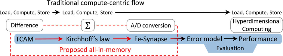
FIGURE 1. Depicts the abstract concept and flow of the used all-in-memory scheme with addition of our Fe-FinFET-based A/D conversion (bottom), and the equivalent conventional digital CMOS alternative (top). The highlighted parts show our contribution and which section we evaluate.
Our novel contributions within this paper are as follows:
1) We propose, design, and accurately simulate the first FeFET-based synapse circuit employed as an ADC. A resolution of N levels requires N FeFETs minimizing the sensing overhead and maintaining a high area efficiency.
2) The FeFET-based sensing circuitry enables an all-in-memory analog system. Not only is the computation done in a Fe-TCAM but also the accumulation of results by exploiting Kirchhoff’s law and the A/D conversion in the FeFET-based synapses.
3) We evaluate the whole system from transistor level all the way up to the application. Our accurate simulations with calibrated models enable us to investigate the impact of process variation at the transistor level on the inference performance at the application level.
1.1 Background
Efficient system design necessitates to cover the whole stack, from a single transistor all the way up to the application level. In this section, the principal concepts of each level are introduced, starting with HDC as the application, FeFET technology at the transistor level, and based on that the Fe-TCAM.
1.1.1 Hyperdimensional Computing
Brain-inspired HDC is a rapidly emerging alternative to traditional machine-learning methods Kanerva (2009). It has been successfully applied to several domains, like language recognition Rahimi et al. (2016b), image classification Kleyko et al. (2017), gesture recognition Rahimi et al. (2016a), wafer map defect pattern classification Genssler and Amrouch (2021), and more (Dua and Graff, 2017; Burrello et al., 2018; Lobov et al., 2018; Kim et al., 2020). Instead of large neural networks, the concept is based on vectors with high dimensionality, with 10,000 being a typical dimension D. The individual components of such a hypervector can have different data types, such as simple bits, integer, or real numbers. Hypervectors are randomly generated and represent real-world data, such as voltage levels, pixels in an image, or letters in the alphabet. To map complex data into hyperspace, multiple simple value-representing hypervectors are combined with three basic operations. The implementation of each operation depends on the components’ data type. The focus of this work is on binary hypervectors; a comparison of other data types is provided in Schlegel et al. (2020).
The first operation is bundling, with which multiple hypervectors are combined into a single hypervector of the same dimension D. Each bit in the resulting hypervector is determined through a majority operation. Ties can be decided randomly or by XOR’ing the first two input hypervectors. The second operation associates two hypervectors together by XOR’ing them, which is called binding. Third, the permutation operation rotates the hypervector, which is useful to encode sequences. All computations can be fully parallelized because each component is independent.
To encode, for example, a text into hyperspace, each letter is first associated with a different randomly-generated hypervector. This association is stored in the Item Memory (IM), a dictionary-like structure. Then, the first n letters are mapped into hyperspace with the IM. The i-th hypervector is permuted i times to encode its position. The permuted hypervectors are bundled into a single hypervector representing this n-gram. These steps are repeated until the whole text is represented by such n-grams. Finally, all n-gram hypervectors are bundled again into a single hypervector encoding the whole text. The process is repeated for different texts from different languages. The association between each hypervector with the language of its text is stored in the Associative Memory (AM).
To classify the language of an unknown text, it is first encoded through the same process into a query hypervector. In the AM, the similarity of the query hypervector to the stored class hypervectors, representing their associated language, is computed. For binary hypervectors, the Hamming distance is employed as a similarity metric. The bits in each position of the query and class hypervector are compared. If they do not match, the distance is increased by one. In other words, the Hamming distance is the number of mismatched bits. The higher the Hamming distance, the less similar are two hypervectors. Hence, the language associated with the class hypervector with the lowest Hamming distance is the classification result.
The achievable inference accuracy depends heavily on the application and the encoding. On the one hand are the underlying operations, such as bundling or Hamming distance computation, application-independent. Consequently, a circuit implementing such an operation is also application-agnostic. On the other hand, impact errors in the underlying hardware applications differently Hernandez-Cane et al. (2021). Thanks to the high dimensionality of the hypervectors, HDC is very robust against noise (Wu et al., 2018; Karunaratne et al., 2020; Hernandez-Cane et al., 2021).
1.1.2 Ferroelectric Field-Effect Transistor
FeFETs based on Hafnium Oxide (HfO2) have emerged as a promising on-chip memory in recent years Böscke et al. (2011). One key advantage over other NVM technologies is their full compatibility with conventional CMOS manufacturing processes (Böscke et al., 2011; Dünkel et al., 2017). HfO2-based FeFET technology does not require new materials or process steps. Since the introduction of 45 nm, HfO2 is used to construct high-κ dielectrics Bohr et al. (2007) and thus the manufacturing processes are mature. A conventional MOSFET (depicted in Figure 2A) can be turned into an NVM transistor by increasing the thickness of the HfO2-based high-κ dielectric layer and doping it with Zirconium (Figure 2B). Due to this enhanceability of the gate stack, conventional Fin Field Effect Transistors (FinFETs) can also be used as base for Ferroelectric FinFETs (Fe-FinFETs) as they are used in this work. Thickening this layer can be omitted for logic transistors without impacting their performance Dünkel et al. (2017). In other words, logic and memory can be manufactured jointly with a single process. Hence, FeFET is a fully CMOS-compatible NVM.
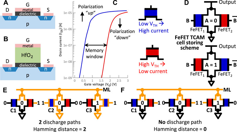
FIGURE 2. (A) Sketch of planar transistor. (B) Sketch of FeFET with a thick HfO2 layer (e.g., 10 nm). (C) ID-VG loop showing two distinguishable states (low − VTH and high−VTH) due to the polarization of the FE layer in the transistor. (D) Single TCAM cell implemented with FeFET and the storing scheme. (E) TCAM block example with two mismatches, forming two discharge paths (i.e., Hamming distance = 2). (F) TCAM block example with no mismatches, wherefore no conducting path is formed.
The HfO2-based FE layer contains dipoles that can be polarized into a desired direction. An electric field through the gate (e.g., VG = ±4 V) flips the polarization of those dipoles to either “up” or “down”. Depending on the direction of the polarization, an applied VG is amplified or dampened. Hence, the transistor exhibits either a low threshold voltage (low−VTH) or a high threshold voltage (high−VTH). This difference in VTH changes the drive current ID, which is sensed at with a low VG (e.g., 0.7 V). Figure 2C demonstrates the difference in ID and the width of the opening between the two opposing states is called “memory window”. Based on this large difference (around six orders of magnitude), two logic states can be distinguished. The polarization is retained for more than 10 years Muller et al. (2012), making the transistor an NVM.
Through the low−VTH and high−VTH states, the FeFET acts as a binary memory. The “up” or “down” polarization is saturated to achieve a reliable operation. A high VG is applied for 1 µs to ensure this saturation (Muller et al., 2012; Dünkel et al., 2017). However, by shortening the time or reducing the voltage, the polarization is only partially saturated (Jerry et al., 2017; Mulaosmanovic et al., 2017). Consequently, an applied VG is partially amplified or dampened, and the FeFET exhibits a VTH between low−VTH and high−VTH. Such an intermediate VTH can be interpreted as a non-binary intermediate state. Jerry et al. experimentally demonstrated 32 states in a single FeFET Jerry et al. (2017). Partial polarization can be achieved by adopting different polarizing schemes based on manipulating voltage through the temporal or amplitude dimension. The FeFET can also be partially polarized by applying multiple pulses to the gate. Figure 3 depicts the relation between those three methods. The ability of a memory cell to represent non-binary states is also known as a multi-level cell (MLC) and has been demonstrated for other memory technologies (Bedeschi et al., 2008; Ahmad et al., 2017; Zahoor et al., 2020).
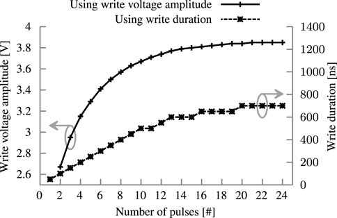
FIGURE 3. Relation of the three different polarization schemes. Write amplitude has a fixed duration of 1 µs, write duration a fixed amplitude of 4 V. The fixed pulse scheme uses 4 V with a 50 ns duration and 50 ns pause in-between pulses.
The main focus in the literature is on n-type FeFET. As shown in Figures 2A,C higher VG increases ID. In p-type FeFET, this relationship is reversed; a higher VG reduces ID. Prototypes featuring both transistor types have been experimentally demonstrated Lederer et al. (2020). Kleimaier et al. demonstrates that the switching behaviour of both transistor types is very similar Kleimaier et al. (2021). The availability of both transistor types offers more possibilities to design circuits for Processing-in-Memory.
1.1.3 Ferroelectric Field-Effect Transistor-Based Ternary Content Addressable Memory
In conventional memory architectures, data is accessed based on an address. In a TCAM, the data itself is supplied and returns the address if the data is present. TCAMs are used already in network routers or CPU caches (Pagiamtzis and Sheikholeslami, 2006; Chang, 2009; Kohonen, 2012) and have been proposed to realize an AM Ni et al. (2019). Traditionally, a single TCAM cell is implemented with two SRAM cells and access logic, in total 16 CMOS-transistors. In contrast, FeFET-based designs require only two FeFETs due to their inherent non-volatility Ni et al. (2019).
Figure 2D depicts an n-type FeFET-based TCAM cell consisting of two FeFETs (FeFET1 and FeFET2). Each TCAM cell is programmed individually by writing the FeFETs in a complementary manner. For instance, to store a logical ‘0’ (A in Figure 2D), FeFET1 is set into the low−VTH state by a 10 µs pulse of +4 V to node B. In contrast, FeFET2 is set into a high − VTH state by a −4 V pulse to
The output of N TCAM cells can be connected as a single Match Lines (MLs) as shown in Figure 4C. N bits of query data are applied in parallel to the N cells. As described above, a cell forms a conducting path in case of a mismatch. The resulting discharge rate of the output ML is proportional to the number of cells reporting a mismatch, as more parallel paths to GND will cause a faster discharge. In other words, the TCAM array calculates the mismatches between the stored and query data and accumulates them as the discharge rate. Calculating the number of mismatches realizes the Hamming distance operation making FeFET-based TCAM arrays an interesting option to implement HDC. In the example in Figure 2E, an N = 3 TCAM array stores “001” and is queried with “010”. Two conducting paths are formed by C2 and C3, resulting in a high discharge rate corresponding to a Hamming distance of two bits. In Figure 2F, the stored and queried data is equal, i.e., Hamming distance of zero. Hence, no conducting paths are formed, and the ML is not discharged.
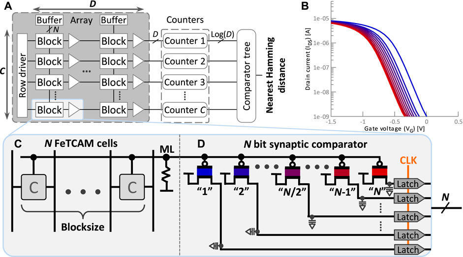
FIGURE 4. (A) Sketch of possible layout with C rows for the class HD vectors each of dimension D cut into blocks of size N Imani et al. (2017). (B) ID-VG plot with the intermediate states of the p-type FeFET synapse. (C) Single Fe-TCAM block with N cells. (D) Our proposed synaptic comparator decoding the analog discharge rate of a N cell TCAM block into digital.
A key challenge of such an implementation is the correlation between the discharge rate and the number of mismatches. The discharge rate saturates and does not scale linearly, limiting the number of mismatches that can be differentiated. To reduce the impact of this non-linearity, the size of a TCAM array is restricted. Long data words, like hypervectors, cannot be stored in a single TCAM array but have to be split into multiple N-bit blocks. Each block is mapped to a separate N-cell array.
1.2 Related Work
Various emerging technologies have been studied to implement HDC. Karunaratne et al. manufactured a chip featuring two phase change memory (PCM) arrays and CMOS logic Karunaratne et al. (2020). For encoding, the query hypervectors were created with a 2-min term strategy where the item hypervectors are stored in the two arrays. For classification, the dot product is computed in a PCM-based AM and a winner-takes-all CMOS-based circuit determines the class index. They did not report specific variation levels but emphasized the robustness of HDC against errors enabling analog PiM inference.
Resistive RAM (ReRAM)-based PiM implementations are frequently proposed as a technology to implement the AM (Imani et al., 2017; Wu et al., 2018; Wu et al., 2018; Liu et al., 2019; Halawani et al., 2021b) exploited the combined variability in CNFET and ReRAM to generate orthogonal item hypervectors. Other components of a HDC system, like the encoder and AM, were also implemented. Even if 78% of the bits in the query hypervector are stuck, the inference accuracy for language classification droped by less than 2% for a binary decision between two languages.
Halawani et al. used an XNOR array to compute the Hamming distance between a query and the stored class hypervectors Halawani et al. (2021b). The XNOR operation was similarly implemented with TCAM cells, with memristors instead of FeFETs. The output voltage response was linear and covered almost the full voltage range from 0 V to VDD for a block size of 16 cells, i.e., 16 bits. Nevertheless, they reported voltage saturation with more cells. To convert the output voltage of the array, they employed a voltage-to-time converter (VTC), generating a pulse with a width corresponding to the XNOR result. The Hamming distances were accumulated through a tree-like structure in the time domain. They demonstrated a whole inference step for a dimension of 1000 bits in a single clock cycle of 10 ns. However, their results are reported without taking variation into account, which impacts ReRAM heavily Fang et al. (2018).
Imani et al. proposed three different AM designs Imani et al. (2017). One was based on regular CMOS memory storing the class hypervectors, an XOR array, binary counters to compute the Hamming distance, and comparators to select the smallest distance. The second design replaced the CMOS memory and XOR array with an ReRAM-based crossbar and a delay-sensing circuit. Due to the non-linearity in this delay, the size of the crossbar, a block, was limited to N = 4 bits. They proposed voltage overscaling to reduce the impact of non-linearity. The third design is fully analog and again used an ReRAM CAM array. Per bit in a class hypervector, a regular CMOS transistor is activated by the query’s bit. If the ReRAM was programmed into a low resistance state (class bit “0”), a conductive path to GND is formed. The sensing circuitry tracked the current, and a loser takes all network outputs the class with the nearest Hamming distance. In their second and third design, Imani et al. considered process variation in their 45 nm technology, which had less of an impact compared to a 14 nm Fe-FinFET considered in this work Imani et al. (2017). Further, their error modeling was static and did not model the connection between different applications and incorrect Hamming distance computations.
Ni et al. and Thomann et al. used a Fe-TCAM block to calculate the Hamming distance in a analog way similar to this work (Ni et al., 2019; Thomann et al., 2021). Both assumed a clocked self-referenced sense amplifier (CSRSA) translating the discharge current into the temporal domain and finally digital values, but no such circuit was presented. While both used ferroelectric-based transistors, Ni et al. used a planar FeFET and Thomann et al. a Fe-FinFET. The specific implementation of the sense amplification scheme with a CSRSA has been unique to these two works, as Imani et al. used a different circuit to achieve a similar result Imani et al. (2017). In this work, a novel Fe-FinFET-based synaptic comparator is proposed to convert the analog results from a TCAM array into the digital domain. Kazemi et al. used a multi-level Fe-TCAM cell to increase bit density further. They discussed the influence of an ADC on several figures of merit yet do not disclose how or what kind of ADC is used Kazemi et al. (2021).
Humood et al. combined ReRAM devices with a conventional flash ADC scheme. In a flash ADC, resistors are used to generate fixed reference voltages to which the input is compared Humood et al. (2019). Humood et al. replaced the resistors with ReRAM devices, which can be programmed, resulting in a post-fabrication tunable ADC. Further, they stated in the future work to also replace the conventional voltage comparators with ReRAM devices, which is presumably very close to the idea we follow in this work.
Hersche et al. investigated the impact of erroneous PCM cells in the AM on the inference accuracy Hersche et al. (2020). They reported an inference accuracy loss of 21.5% for language classification at a failure rate of 48.5%. Their proposed unsupervised method recreates the class hypervectors from a second training data set. The accuracy was almost fully restored. Their error model considered only faults in the underlying memory of the AM, not in the computations of the Hamming distance.
2 Materials and Methods
This section describes the structure and concept of an AM build with a FeFET-based synaptic comparator connected to Fe-TCAM cells. Those cells are grouped into blocks and store N bits of the class hypervector as shown in Figure 4. When queried, the mismatching cells form a conducting path lowering the voltage of the ML. A FeFET-based synaptic comparator, described in Section 2.1, is connected to this ML. In contrast to an n-type FeFET, the reduction in voltage causes this p-type FeFET to open and thus charge a capacitor. The speed of the charging depends on the FeFET’s programmed VTH. If, after a sampling period, the capacitor’s charge is above a threshold, then a certain number of Fe-TCAM cells are mismatched; in other words, the query has at least a certain Hamming distance to the class hypervector. To increase the resolution from a binary threshold with one synapse to the actual Hamming distance, N synapses are combined into the N-way synaptic comparator described in Section 2.2. The joined Fe-TCAM and N-way comparator are introduced in Section 2.3, whole AM circuit is described in Section 2.4 and the error modeling in Section 2.5.
2.1 Ferroelectric Field-Effect Transistor-Based Synapse
The neuromorphic-computing community shaped the notion of a synapse and defined it from an electrical engineering perspective as a conductance modulatable circuit element (Jerry et al., 2017; Mulaosmanovic et al., 2017). A FeFET’s VTH can be modulated by partially polarizing domains in the FE layer, turning it into a non-volatile conductance modulatable circuit element Jerry et al. (2017). This concept of a multi-level cell is explained in detail in Section 1.1.2. In a FeFET, the different levels of saturation correspond to a different VTH. As depicted in Figure 2C for two different VTH, the VTH determines the drive current ID when a VG is applied. If the FeFET is used as a memory cell, then ID is measured and represents the cell’s state or stored value. However, the FeFET is not used as a memory cell in this work. Instead, it is employed as a programmable non-binary switch.
The FeFET is “programmed” the same way as a multi-level memory cell by saturating the polarization of the FE layer to distinct levels. The resulting ID − VG curves are shown in Figure 4B. Note that in this work, a p-type FeFET is used, which has been experimentally demonstrated recently and gains more attention Lederer et al. (2020). In contrast to the more common n-type, the p-type is in the active state at VG = 0 V and in the cut-off state when VG is increased above VTH. However, as the FeFET is employed as a non-binary switch, it does not have these two states but is always considered active. Further, VG is not fixed to a predefined Vread. Instead, VG is treated as a variable input controlling the output ID. Connected to the drain is a capacitor that is constantly being charged during a query operation. The charge rate depends on ID, which in turn depends on both, VG (non-binary) and VTH (the “programming”).
In this work, the purpose of a FeFET-based synapse is to measure if VG is above a programmable threshold. To derive this binary decision from the charge of the capacitor, a D latch is connected. By charging the capacitor, the voltage at the input of the latch VCap is increased and approaches VDD. After the sampling period tsample, the latch activates and captures a logical “1” if VCap is above approximately VDD/2, otherwise a logical “0”. In other words, the capacitor and latch discretize the analog FeFET-based synapse. This logical value captured by the latch is later used for further processing. After the latch has captured the value, the capacitor is discharged and reset for the next query operation.
Our FeFET-based synapse circuit features various tuneable parameters, including 1) the metal workfunction of the FeFET itself, 2) the resistor connecting supply voltage and ML, 3) the size of the capacitor, and 4) the sampling period tsample. The parameters impact the energy, area, and accuracy of the circuit. The metal workfunction 1) of a FeFET-based synapse is a tradeoff between its leakage and the adaptation to voltages coming from the ML. With the metal workfunction parameter, the ID−VG characteristic can be shifted horizontally (i.e., the VTH) but is permanent after fabrication. On the one side, it is used to shift the memory window (like in Figure 2C) such that it matches the input range coming from the ML and is capable of distinguishing them. On the flip side, the transistor has to be able to produce sufficient current to charge the capacitor fast enough, which may lead to a leaky transistor (ID−VG curve is close to 0 V in Figure 4B). The consequence of the metal workfunction engineering on the energy consumption is discussed in Section 3.4. The other synapse parameters (resistor, capacitor, and sampling period) are discussed in the context of the AM and whole ADC circuit in the following sections.
2.2 N-Way Synaptic Comparator
A single FeFET-based synapse can be programmed to measure if VG is above a threshold. This threshold can be changed at runtime by reprogramming it, and a single synapse could differentiate between different thresholds. However, reprogramming and measuring take time and energy. Alternatively, N FeFET-based synapses are combined into a single circuit as shown in 4D. The synapses are programmed with an increasing VTH so that synapse “1” has the lowest and synapse “N” the highest VTH. Hence, similar to a flash ADC Kumar and Ch (2020), each synapse detects a different threshold. All gates of the FeFET-based synapses are connected and subject to the same VG. Depending on their programmed VTH, each capacitor is charged and VCap changes at a different rate. After the sampling period tsample, the number of D latches storing a logical “1” correlates with the voltage level of VG.
2.3 All-in-Memory Hamming Distance Computation
A Fe-TCAM block, described in Section 1.1.3 and depicted in Figure 4C, is used to compute the Hamming distance between N bits of the class hypervector and N bits of the query hypervector. For each mismatching bit, a Fe-TCAM cell establishes a conducting path from the ML to GND. The more mismatches occur, the lower is the voltage of the match line VML. This VML is measured with the proposed N-way synaptic comparator. For that purpose, the ML is connected to the gates of the FeFET-based synapses, i.e., VML = VG. Since the synaptic comparator is implemented based on p-type FeFETs, a reduction in VML (VG) will activate the synapses. The lower VML (VG) is, the more synapses are activated, and the higher the Hamming distance is. Hence, there is a direct correlation between the mismatches in the Fe-TCAM block and the Hamming distance reported by the synaptic comparator. After the sampling period tsample, N-many latches store a logical “1” representing a Hamming distance of N.
Determining the drive current of each FeFET-based synapse at a given VG is an important step during the design of the circuit. The drive current determines the time it takes the synapse to charge the connected capacitor. Only if VCap exceeds VDD/2 does the D latch store “1” and signals the synapses activation. All the drive currents of the FeFET-based synapses have to be carefully calibrated so that the mismatch level is equal to the number of activated synapses. In the first step of this calibration, all mismatch levels are simulated in Simulation with Integrated Circuit Emphasis (SPICE) individually to extract the respective VML of the Fe-TCAM array. Second, for each extracted VML (VG), a synapse’s VTH has to be found at which its drive current is sufficient to charge the capacitor and activate. In this work, the voltage amplitude-based programming scheme is employed and thus the write voltage is swept to explore VTH. The swept write voltage ranges from 2.5 to 4.0 V, often used values in the literature (Jerry et al., 2017; Luo et al., 2019; Xiao et al., 2019), with a constant duration of 1 µs. As a final step, the explorations of VML and write voltage are combined so that the mismatch level is equal to the number of activated synapses.
The calibration is summarized in Figure 5. The write voltage is swept from 2.5 to 4.0 V in 0.1 V steps for a single synapse. The 10-bit Fe-TCAM array is configured to output a mismatch level of one. Despite the high VML (compare Figure 6), the p-type FeFET-based synapse still drives enough current to sufficiently charge the capacitor at the sampling time. By increasing the write voltage and thus VTH, the synapse drives less current. After polarizing being polarized with 3.1 V, it does not activate with the mismatch level of one. At this point, the mismatch level is increased by one and the synapse activates again. The write voltage sweep continues until a mismatch level of ten is reached creating the staircase-like pattern.
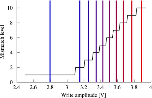
FIGURE 5. Mapping of the write amplitude to the output Hamming distance used for calibration of the synaptic comparator. Vertical lines indicate the selected amplitudes that maximize margins.
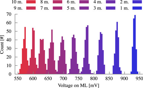
FIGURE 6. Historgram of the VML distribution at different mismatch levels for a block size of 10 bit. The nominal VML for no mismatches is 1.0 V.
In the SPICE simulations, ideal multiplexers are employed to decouple the ML from the individual gates of the FeFETs during the write scheme. An ideal multiplexer does not interfere with the circuit operation in the computation step and does not affect the reported energies. This limitation is discussed in Section 4. For an actual implementation, double-gated FeFETs are available and can be used to decouple the write from read port Kim et al. (2021). Such a scheme would not impact the reported results significantly.
One challenge imposed by the Fe-TCAM block is the non-linearity in the VML reduction. The ΔVML for two neighboring Hamming distances is exponentially decreasing with an increase in the Hamming distance. Due to the limited resolution of the synaptic comparator, two too similar VG can cause errors. To counteract the non-linearity, a resistor is added between the ML and VDD charging the ML. Furthermore, this gives the designer control and tunability of the VML distribution. This and interaction with other parameters is discussed in Section 3.2.1.
Another design parameter of the proposed circuit is the size of the capacitor and the sampling period tsample. A larger capacitance increases the charging time and consequently requires an increase in tsample. On the one hand, such an increase improves the margins between the different synapses reducing the likelihood of errors. On the other hand, the whole circuit has a high leakage power, and a higher tsample increases the total energy consumption. This tradeoff is explored in Section 3.2.2.
The described circuit is referred to as an N-bit block. For large N, the non-linearity renders high Hamming distances indistinguishable. To reduce unnecessary area and energy costs, the concept of precision is introduced. No synapse is deployed to detect such indistinguishable Hamming distances. Hence, the number of synapses NSynaptic is smaller than the bits stored by the TCAMNTCAM. This creates a fundamental compromise between block size and precision. Two implementations of this concept are possible. In the first, the highest detectable Hamming distance is limited to the NSynaptic levels the synaptic comparator offers instead of the full NTCAM bits. The FeFET-based synapses are programmed to differentiate only NSynaptic levels of Hamming distance. If the number of mismatches on the Fe-TCAM block is higher than NSynaptic, then these values are limited to NSynaptic. The maximum expected error is NTCAM−NSynaptic bits in Hamming distance. Second, the spacing between the FeFET-based synapses’ VTH is increased so that the minimum and maximum VTH correspond to a Hamming distance of one and NTCAM, respectively. Intermediate distances are reported as a neighboring one with a maximum expected error of NTCAM/NSynaptic bits in Hamming distance. The actual inference accuracy loss of both schemes is application-dependent since the similarity of their hypervectors determines the final accuracy loss.
2.4 Our Proposed Ferroelectric Field-Effect Transistor-Based Associative Memory
The analog Hamming distance computation results in a number of logical “1”s stored in the D latches of a block, forming an N-bit subsection of a single class hypervector. Hence, for each class, D/N blocks are required. Accumulating the block results gives the total Hamming distance of the whole query to the class hypervector. Such an accumulation is performed by the priority blocks followed by adders, which are not modeled in this work but can be implemented as shown in the literature Imani et al. (2017). The priority blocks interpret the highest firing D latch and translate it into a binary encoded number. To compute for C classes in parallel, the AM features a total of C*(D/N) blocks and C accumulation units. Lastly, a digital comparator outputs the index of the lowest Hamming distance as depicted in Figure 4A. This index has been associated with a class label during setup and is the result of the inference.
2.5 Process Variation Effects and Error Probability Modeling
To accurately evaluate our proposed circuit, the industry standard BSIM-CMG Chauhan et al. (2015) compact model is used. The employed transistor model is calibrated to reproduce the production-quality Intel 14 nm FinFET process Natarajan et al. (2014). Measurements and calibrated results are in excellent agreement, including transistor characteristics, in ID−VG as well as ID−VD for both nFinFET and pFinFET (Figures 7A,B). Furthermore, transistor-to-transistor variability is captured by the model through calibration against the measurements Amrouch et al. (2020). For a comprehensive representation of process variation, all important sources of manufacturing variability (gate work function, fin height, fin thickness, channel length, and effective oxide thickness) are modeled, and benchmarked against measurements from the same targeted technology (i.e., Intel 14 nm FinFET). The compact model and SPICE Monte-Carlo simulations build the foundation to calibrate the standard deviations for each mentioned source of variability. Again, excellent agreement is demonstrated in the ION vs. IOFF results through Monte-Carlo SPICE simulations (Figures 7C,D).
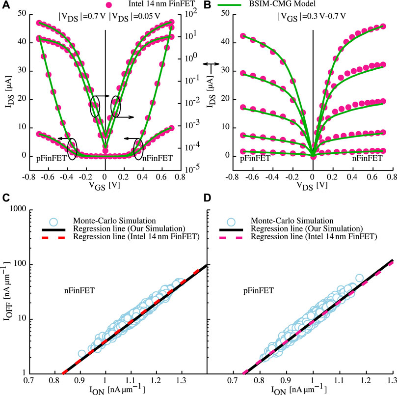
FIGURE 7. Calibration and validation of the compact model against Intel 14 nm FinFET measurements extracted from Natarajan et al. (2014). For all different biasing conditions both nMOS and pMOS are considered (A,B). Similarly, variability is validated against Intel 14 nm FinFET, again for nMOS and pMOS in (C,D), respectively. Details on device and variability calibrations are available in \cite{TCASI20_2} Amrouch et al. (2020).
As the transition from a regular MOSFET to FeFET is enhancing the gate stack, the solid foundation of the FinFET described previously is inherited by the used Fe-FinFET. The Preisach model is incorporated into the compact model to extend the FinFET with the ferroelectric behavior Ni et al. (2018). By assuming independent domains within the FE layer and the unique history tracking of the hysteresis loop, the Fe-FinFET characteristics are captured. As a result, the multi-domain FE model reproduces qualitatively the experimentally observed binary and multi-level properties of Fe-FinFET. The ferroelectric specific parameters have been calibrated against measurements of a ferroelectric capacitor Gupta et al. (2020). Not considered in this work are the variation sources introduced by the FE layer itself (saturation polarization, remnant polarization, and coercive field), resulting in a more optimistic analysis Ni et al. (2020). However, the underlying FinFET model includes variability enabling the analysis of the circuit under the influence of process variation.
Due to variability, the VTH and consequently the drive current of the Fe-FinFETs is altered. This affects the proposed circuit twofold since the two subcircuits both employ Fe-FinFETs. For one, the Fe-TCAM block’s results form the Hamming distance computation as different voltage levels on the ML. Changing the drive current of the Fe-FinFETs in the Fe-TCAM cells also changes the VML. As the VML is used to activate the synapses of the comparator, the charging speed of the capacitor is affected. A reduction in VML can therefore prevent the activation of the D latch, which incorrectly reports a “0” instead of a “1”. Analogously is an incorrect Hamming distance computed if the VML is too high, charging the capacitor too fast, and incorrectly activating the synapse. The synaptic comparator represents the computed Hamming distance in a digital form through the D latches. The Hamming distance is determined by the highest distance represented by any of the activated synapses. This interpretation of the outputs by the comparators is common practice in conventional flash ADC designs, wherefore we adopt it here as well Kumar and Ch (2020). Due to the variability-induced errors, the highest activated synapse is not necessarily the Hamming distance. For example, the distance is three, but the synapses representing “1”, “2”, and “4” are activated. The result is considered to be “4” as the highest is prioritized.
The second subcircuit impacted by variation are the Fe-FinFET-based synapses themselves. Similarly, the drive current, thus the charging speed, and the ultimately computed Hamming distance are affected. Even with an ideal VML (nominal Fe-TCAM cells), variability in the comparator can cause incorrect Hamming distance results through similar effects described above. As the Fe-TCAM block and the synaptic comparator work in unison, variation in one affects the other and vice versa. Therefore, the effects of process variation are jointly analyzed using Monte-Carlo SPICE simulations of the whole circuit.
For the error model, all N possible mismatch levels of the Fe-TCAM block are simulated with 1,000 samples each. For each mismatch level, the potentially incorrect Hamming distances reported by the comparator are collected. Normalizing these results yields a joint probability distribution describing the likelihood of input mismatch level X being reported as Hamming distance Y. Such a 2D matrix fully describes the error model of an N-bit block with a comparator. The circuit-level model is used in an application-level analysis to calculate the inference accuracy for various benchmarks. Class and query hypervectors are created from the data sets. Each class hypervector is partitioned and stored into D/N N-bit blocks. For each block, the correct Hamming distances between the stored class to all queries are computed. The error model is queried with the correct Hamming distance to emulate the expected variation-induced errors of the circuit. The potentially incorrect Hamming distances are summed up for all classes. If the induced error is large enough, the query hypervector appears to be more similar to another class than initially computed. Such a change is likely to result in a wrong inference since the baseline HDC model correctly infers the large majority of queries. The loss in inference accuracy shown in Figure 8 is calculated against the inference accuracy of this baseline HDC model with respect to the dimension.
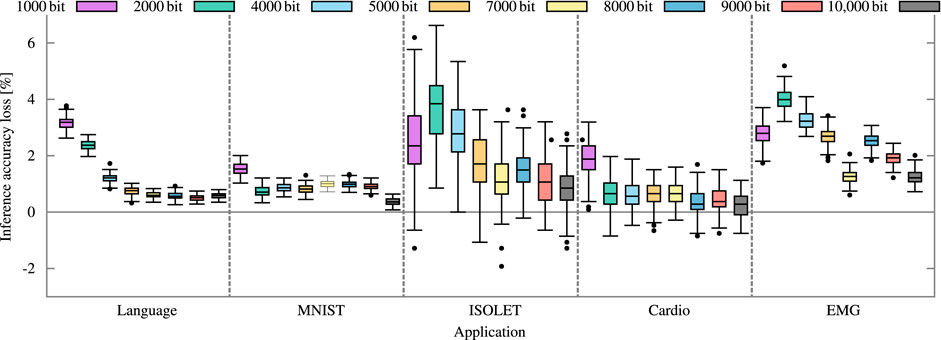
FIGURE 8. Inference accuracy loss of five different applications based on the 10-bit block with 10-bit precision error model. We use language recognition, image classification (MNIST), gesture detection (EMG), voice recognition (ISOLET), and heart disease detection (CARDIO).
The whole computation of the inference accuracy loss is repeated 100 times to minimize the inherent randomness of the error model. This number of repetitions is sufficient to observe major and minor trends in the results with a high confidence. According to the Z-test and Bartlett’s test, the distribution of the results from 100 repetitions is statistically equal to the distribution of 1,000 repetitions using the example of language recognition.
3 Results
Various parameters can be tuned to improve and explore the proposed circuit. Furthermore, the variability-induced errors are modeled at circuit level and used at the application level to evaluate the impact on the inference accuracy. The circuit is evaluated at a capacity of 5 fF, tsample of 1 ns, and resistances of 4.3, 2, 1.3 kΩ for a block with 5 bit, 10 bit, 15 bit, respectively.
3.1 Error Probability Model
Each pair of query and class hypervector has a defined Hamming distance, a part of which is computed in each block. However, due to process variation, a block does not always compute the correct distance. Instead, the error model assigns probabilities to compute an (incorrect) Hamming distance for a given mismatch level input. Such a model is visualized as a stacked bar chart in Figure 9 for a 10-bit block. The marked corridor in the middle represents a correct computation. In the case of zero mismatches, no Fe-TCAM conducts, the VML is not reduced and thus no capacitor is charged. Errors will not occur, since the margins are too high. As the mismatch level increases, the shrinking margins (due to non-linearity) cause the probability distribution for the correct result to shrink, leading to a funnel-like effect. The likelihood of a wrong result is summarized in the error probability graph in Figure 10. Developing such an error model bridges the gap between the transistor and application level. The model allows to analyze the impact of changes in the underlying hardware on the inference.
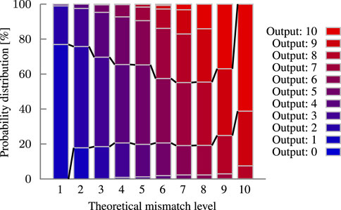
FIGURE 9. Probability distribution modeling the output of the synaptic comparator for a given input under process variation. The funnel-like shape by the probability mass of the correct outputs is highlighted with the black lines. 10-bit block with a precision of 10 bit.
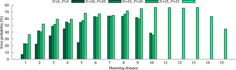
FIGURE 10. Error probability of our four circuit configurations. The error probability is the summary of how likely it is to get the wrong result for a given input. Analysis is done at respective block size (N) and precision (P).
3.2 Impact of Circuit Tuning Parameters
The impact of four circuit parameters is investigated in this work. Each offers tradeoffs that can be exploited by circuit designers to optimize for their specific needs.
3.2.1 Impact of the Resistance
Reducing the resistance value of the resistor between the ML and GND has the strongest influence of the non-linearity of the Fe-TCAM array. As shown in Figure 11, a low value of 0.5 kΩ creates an almost linear dependency between Hamming distance and VML (R2 = 0.9985). In contrast, 10 kΩ exhibits a reciprocal relationship and R2 = 0.9085. However, the drawback of a small resistance is the actual differences in VML between the Hamming distances. For 0.5 kΩ, the total ΔVML is 135 mV, the minimum and average ΔVML between Hamming distances is 13 and 15 mV, respectively. For 10 kΩ, the total ΔVML is 592 mV, the minimum and average ΔVML is 22 and 66 mV, respectively. However, the resistance cannot be arbitrarily increased because the ΔVML will converge to 0 V for the higher Hamming distances. In summary, the high resistance offer a 70% higher minimum and 340% higher ΔVML margin on average. But the isolated analysis is insufficient as it leaves the other parts of the circuit out of the picture. With higher resistances, the staircase in Figure 5 shifts to the right and pushes stairs over the 4 V write voltage boundary. This issue can be tackled by engineering the metal work-function of the Fe-FinFETs constructing the synapses to shift the memory window such that it fits the VML range. The metal work-function value was chosen beforehand and the tuning of the other parameters is done after.
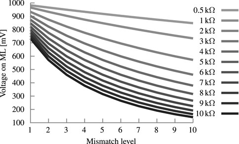
FIGURE 11. Analysis of the resistance connecting the supply voltage and the ML. It shows the development of VML over the different mismatch levels for a block size of 10 bit.
3.2.2 Impact of the Capacitance
The proposed circuit is evaluated with two different capacities, 1000 fF and 5 fF. To ensure proper functionality, tsample is set to 100 and 1 ns, respectively. The higher capacity and tsample should offer more margins to compensate for variation. However, the average error probability is only reduced by 5% from 45.65 to 43.43% for a 10-bit block. The average inference accuracy loss at D = 10,000 is reduced by 9% from 0.576 to 0.525%. The cost of the 9% improvement is a 100× larger delay and almost 100× higher energy consumption.
3.2.3 FeTCAM Block Size
The size of a block is a tradeoff between inference accuracy and energy. In larger blocks, more mismatch levels have to be distinguished within the same voltage range. The decreased margins between the levels make the comparator more susceptible to variation. The impact of this decrease on four circuit configurations is demonstrated in Figure 10 by the higher error probability. At the application level, the loss in inference accuracy increases proportionally to the error probability, shown in Figure 12 for the example of language recognition. Utilizing three times as many 5-bit blocks as 15-bit blocks improves the accuracy by 1.6 to 0.2 percentage points for dimensions from 1000 to 10000 bits, respectively. The energy consumption increases by 6.8% on average, additional overhead for the extra counters is not yet considered. Another limit to the block size is the non-linearity of the discharge rate which can be partially counteracted by scaling the resistor (Section 3.2.1).
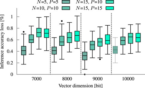
FIGURE 12. Influence of block size and precision on inference accuracy at the example of the Language. Analysis is done at respective block size (N) and precision (P).
3.2.4 Block Precision
In HDC, hypervectors of the same class should have the smallest Hamming distance among each other. By finding this smallest distance, a query hypervector is assigned to its matching class. Consequently, the query has a high distance to other class hypervectors. Thus, the computed Hamming distance in a block will be on average half of the block size. Hence, it is more important to be accurate in the lower than in the upper distances. This HDC-specific property aligns well with the concept of precision. Reducing the precision reduces the hardware cost and increases the margins towards a lower error probability (compare Figure 10). Figure 12 shows the marginal impact on the inference accuracy loss of language recognition through the precision reduction.
3.3 Impact of Process Variation on Inference Accuracy
The Fe-TCAM array and the Fe-FinFET-based synaptic comparator are both impacted by processes variation. To analyze their individual contribution to the error probability and by extension inference accuracy, variation is disable in the other subcircuit. The methodology described in Section 2.5 is applied to extract the error model. First, process variation is only considered in the Fe-TCAM array. The variations in the underlying electrical properties change VG for each Fe-FinFET. Consequently, their effect on VML in case of a mismatch changes. The full circuit with a 10-bit block is simulated for each mismatch level 200 times. The distribution of VML is depicted in Figure 6. The overlap for a mismatch level of six and lower is insignificant to non-existent. Thus, in combination with an idealistic conversion, the Fe-TCAM subcircuit has little to no errors. The probability of an error is given in Figure 13A. For mismatch levels of six to ten, the overlap increases due to the non-linearity. An overlap indicates that two fabricated devices can report the same VML for two different mismatch levels due to variation. An ADC has fixed threshold voltages across all devices. In one of the fabricated devices, the ADC inadvertently reports an incorrect mismatch level, a variation-induced error occurred. The probability of such an error is captured in Figure 13D, which is very low with at most 6%. Hence, the loss in inference accuracy for language recognition is limited to 0.48%.
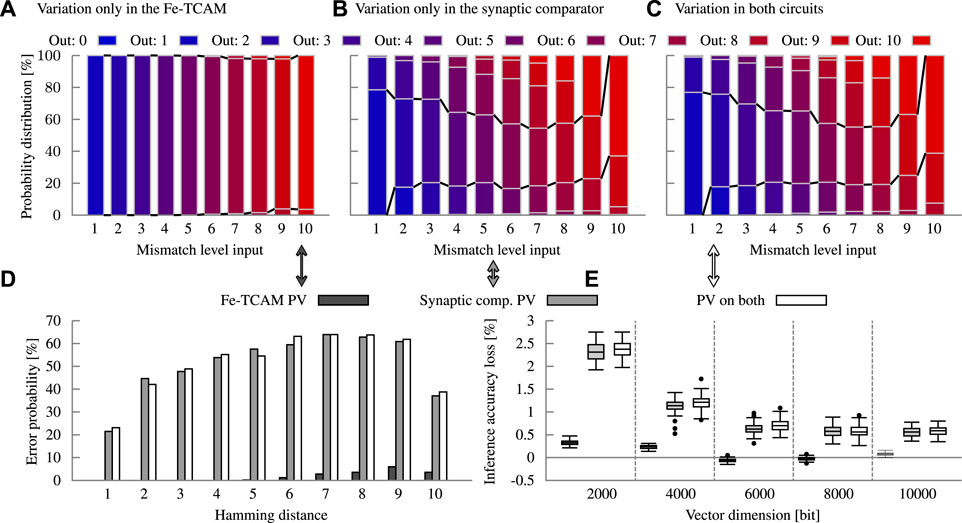
FIGURE 13. Analysis of the impact of variation on the two main components in our circuit and its consequences. Variability in the Fe-TCAM block results in almost no erroneous calculations whereas the synaptic comparator is the main source of errors when affected by variation, as shown in (A,B), respectively. (C) shows the error model with both components under process variation (PV). (D) shows the summary in form of the error probability. (E) finally shows the resulting inference accuracy losses at the example of language recognition. All the analyses are done with a 10-bit Fe-TCAM block at a precision of 10 bit.
In the Fe-FinFET-based synaptic comparator, the input voltage range is with 440 mV approximately half as wide as for the Fe-TCAM. Additionally, the synapses have less distinct VTH levels. Both factors combined result in significantly smaller margins making the comparator more susceptible to variation. The error probability reaches 64% and averages 51%. Despite these high numbers, the inference accuracy for language recognition is reduced by 3.7% at most, for dimensions above 5000 bits by 0.6% on average.
Process variation is considered jointly for both subcircuits in Figure 8 for five different applications. The joined error model does not result in significantly different inference accuracy losses since the Fe-TCAM array contributes little. The solid bars are the mean, and the error bars represent the minimum and maximum, respectively. The different applications react differently to the errors induced by process variation. The variance is large with several outliers and the inference accuracy loss correlates only slightly with dimension. Figure 8 also shows some negative losses indicating an accuracy gain, which is indeed possible due to the randomness in the error model. A detailed analysis of the accuracy gain and the high variance of some applications is not within the scope of this work.
3.4 Energy Consumption Analysis
The higher the Hamming distance, the more Fe-TCAM cells form together a conducting path. The current ION flowing through those cells is the major source of energy consumption. Even though a larger block has more cells, if they are not activated then they do not contribute in a significant way due to their low IOFF, as depicted in Figure 14. For the same Hamming distance, the configuration with N = 10 consumes virtually the same energy as N = 15 for a single query operation. A second contributor is the energy spent charging the capacitors. Hence, the number of synapses (i.e., the precision) is another important parameter. For N = 15, the increase in energy consumption from precision ten to fifteen by 44 fJ on average is due to the five additional capacitors. This difference increases with the Hamming distance from 16 fJ to 75 fJ because the Fe-FinFET-based synapses have a lower VTH charging more capacitors sooner. However, the loss in inference accuracy is marginal as described in Section 3.2.3.
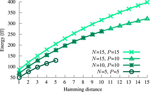
FIGURE 14. Energy consumption of the Fe-TCAM block with synaptic comparator at given circuit configuration. Analysis is done at respective block size (N) and precision (P).
Despite the increase in energy for larger blocks, they are more efficient per bit. With N = 15 as a baseline, 5-bit or 10-bit blocks consume on average 6.8% or 1.9% more energy, respectively. Not considered are the additional counters to accumulate the results from all the blocks. However, during hold, the circuit can be power gated, as Fe-TCAM blocks and synapses are both non-volatile and retain their data and programmed VTH, respectively.
To put the results into context, a similar circuit based on traditional CMOS is simulated. N regular XOR gates and an adder tree with respective depth form a special function block in a CPU. In such a scenario, the energy consumed through the memory access by the CPU has to be considered as well. Reading 512bits from the L2 cache consumes 288 pJ, or scaled to 10 bits 5,625 fJ (ITRS 32 nm, Chen et al. (2012)). The actual computation of 10-bit block consumes 118 fJ compared to 186 fJ of the proposed Fe-FinFET-based circuit. The cache access alone costs an order of magnitude more energy than the actual computation. Thus, achieving the same order of magnitude for the computation compared to a CMOS implementation will lead to massive savings through the PiM scheme.
3.5 Area Requirements
Each N-bit block consists of two parts, the Fe-TCAM block and the synaptic comparator. The number of transistors per block scales linearly with its size N, in other words the number of bits. The Fe-TCAM requires two Fe-FinFETs per bit, the synaptic comparator one Fe-FinFET, one capacitor, and 18 CMOS transistors for the D latch. Hence, the total number of transistors is 21*N plus one resistor. For example, a 5-bit block needs 10 Fe-FinFET for the Fe-TCAM cells, 5 Fe-FinFET for the synaptic comparator, and 90 CMOS transistors for the D latches, giving in total 105 transistors. The main contributor are the CMOS-based D latches in the comparator. As discussed in Section 3.2.4, reducing the precision does not impact the inference accuracy significantly and at the same time offers the most potential to reduce the area requirements. Given a precision P, the total number of transistors is 2*N + 19*P. For a 15-bit block, a reduced precision of 10 saves 30% in area.
3.6 Comparison With Related Work
Imani et al. used a conventional sense amplifier which translated the discharge rate into the temporal domain and sampled the respective output with different timings Imani et al. (2017). The sampling times are generated with a seed clock signal and parallel buffer chains (details in Section 3.5) of various lengths. This approach leads to a linear progression in sampling times as the number of chained buffers is discrete. To cope with the issue of non-linearity, the block size is limited to just 4 bits, obtaining a roughly linear output relation of the signals. This reduces the implementation complexity of the circuit, as there is no need to adapt to the non-linear behavior. However, keeping the block size small enough (e.g., 4 bits) to be able to assume linearity, the scaleability is strongly limited as discussed in Section 3.5. Due to the use of different technology nodes, a comparison to their proposed layout is only possible by counting the number of used transistors. For an N-bit block, decoding the Hamming distance requires 6N + 2N(N−1) transistors Imani et al. (2017). The chained buffers to delay the clock signal cause the quadratic relation. In contrast, the proposed circuit in this work scales linearly and thus requires less transistors for N > = 8.
In (Ni et al., 2019; Thomann et al., 2021) a similar approach is used as in Imani et al. (2017) with a CSRSA, which also translates the discharge rate into the temporal domain. In these two works the conversion of the analog result to a digital one is not discussed. In case a regular ADC (e.g., SAR-ADC) is applicable, based on their results, such an ADC would need a sampling rate between 10 and 100 GHz.
Halawani et al. employed a Voltage-to-Time-Converter (VTC) to translates the Hamming distance result encoded as voltage level into a voltage pulse of proportional width Halawani et al. (2021a). The VTC with 12T is a constant hardware cost per block aside from the ReRAM elements for the TCAM cells. The pulses are accumulated over the row with a tree-like structure, and the winning class is found. The accumulation happens in the time-based dimension, which Halawani et al. claim is more variation and noise resilient compared to the voltage-(/analog)-domain where the signal to noise ratio is degraded due to voltage scaling. The hardware cost of a single block is the ReRAM elements plus the VTC compared to the Fe-TCAM cells and the synaptic comparator in this work. As both ReRAM and Fe-TCAM use two elements per cell, this work does not scale as well due to the more complex comparator. Their VTC requires twelve transistors whereas the proposed synaptic comparator uses N Fe-FinFETs plus 18*N CMOS transistors. They report that the whole inference takes a in single clock cycle of 10 ns (10 classes, D = 1,000, block size of 16 bits). In this work, the results on the block level are present after tsample which is 1 ns, giving a similar time complexity considering the accumulation and winner selection. Unfortunately, variability is not discussed by Halawani et al. Therefore, their claim of better robustness against variation and noise cannot be evaluated.
A state-of-the-art flash ADC design Kumar and Ch (2020) employs ten CMOS transistors per comparator, four per NAND, and M + M/2 for the priority encoder with M as the number of bits in the output. A 4-bit (M = 4) flash ADC has 24 = 16 comparators and thus requires 320 CMOS transistors in total (20 per comparator). To achieve the same output resolution, our proposed Fe-FinFET-based design requires 16 synaptic comparators. Each consists of one Fe-FinFET and 18 CMOS transistors for a total of 304 transistors, a 5% reduction. Hence, both designs require a similar number of transistors with a slight advantage for our proposed design. A fair comparison of energy and latency requires both designs to be implemented in the same technology, in this work 14 nm FinFET. In the literature, most designs employ either larger technology nodes (e.g., 180 nm Kumar and Ch (2020) or use different ADC designs with a higher resolution (e.g., 16-bit SAR-ADC Luu et al. (2018). Comparing our SPICE simulation results with measurements from a fabricated device Nam and Cho (2021) is also misleading since the latter contains layout parasitics and other factors not considered by our simulations. Further, the employed 14 nm FinFET model, which is calibrated to replicate measurements from Intel, is different from other manufactures’ 14 nm technology and adds additional uncertainty to a comparison. In summary, energy and latency cannot be compared in a fair way because no Intel 14 nm 4-bit flash ADC design is publicly available.
4 Discussion
Process variation is the main source of errors in the proposed circuit because it exceeds the available margins between the mismatch levels. Hence, reducing variation will also reduce the loss in inference accuracy. A back-gated FeFET, produced with the recently proposed channel-last fabrication technique, has demonstrated reduced variation at lower write voltages and better scalability at fast programming speeds Sharma et al. (2020). Yet, in contrast to mature CMOS, FeFET technology is still in its infancy. Like any other emerging technology, it suffers from increased variation in those early stages. Nevertheless, it is now the right time to investigate such technologies and harvest their efficiency gains. Hence, HW/SW codesign is key to ensure the applicability of the proposed concepts in the face of further technological development. Our cross-layer modeling linking the underlying technology with running applications is indispensable towards increasing the robustness against errors. Additionally, dedicated hypervector encoding methods have to be investigated, which target specific error pattern stemming from the block and precision concept.
In the presented experiments, the variation in the thickness of the FE layer is not considered due to the lack of publicly available variability measurements for advanced Fe-FinFET. To provide a perspective on the potential impact, we consider a conservative scenario in which the variation in the FE thickness (TFE), remnant polarization (PR), and coercive field (EC) is 1% (σ/μ). This, in turn, represents about 3× more variation compared to the metal work-function (0.34%). Figure 15 summarizes the results for language recognition with a block size of 10 bits and a precision of 10. With 1% variation in the FE layer, the error probability increases by up to 7.7%. This is reflected in the inference accuracy loss, which increases notability by up to 0.3 p.p. for a dimension of 2000 bits (2.37–2.67%). For higher dimensions, the absolute loss does not increase as much, at 10000 bits from 0.58 to 0.64%. The relative increase in inference accuracy loss compared the FinFET baseline is about 13% without a correlation with dimension.
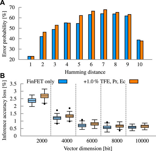
FIGURE 15. Ferro variability analysis through variation of ferro thickness (TFE), remnant polarization (PR) and coercive field (EC) on top of the variation of the underlying FinFET. (A) Error probability of the different variation setups. (B) Inference accuracy loss due to the injected error of the variation setups.
Compared to CMOS-based SRAM, FeFET has low endurance. The reported numbers in the literature vary widely from 105 Mulaosmanovic et al. (2019), over 1010 Tan et al. (2021) to 1012 Sharma et al. (2020) program/erase cycles. However, the FeFETs in the proposed circuit experience only one full programming cycle during setup. Yet, every query operation to the Fe-TCAM is similar to a full read. The sensing of the ADC is similar to a read, although with lower voltages. Chatterjee et al. does not report a break down of the FeFET after 1010 reads Chatterjee et al. (2017). Nevertheless, further studies on the endurance of Fe-TCAM and FeFET-based synapses are necessary.
As discussed in Section 1.1.2, three methods to change the polarization of a FeFET are known. One of them applies repeated pulses, which is also known as accumulated switching Mulaosmanovic et al. (2020). Mulaosmanovic et al. reported a change in VTH after an accumulated pulse time of 100 ms which corresponds to 108 query operations at 1 ns for a voltage of 1 V. Their results suggest that the Fe-TCAM has to be refreshed from time to time. The implications for the synapses are unclear. The voltage is lower than 1 V, but the non-binary synapses are more susceptible to changes of VTH than a binary Fe-TCAM.
In the experiments, an ideal MUX, in which only the behavioral function is simulated, is assumed. For a proper implementation, the required multiplexer circuit should be able to select a certain voltage level from multiple received voltage rails. Such a MUX circuit might be different from a conventional MUX circuit, which is typically used to select a certain logic value among different received logic inputs. Nevertheless, to quantify the potential impact of the additional capacitance induced by MUXes, the capacitance associated with a single convectional MUX is ∼ 0.6 fF using the employed 14 nm FinFET technology node. This additional capacitance of 6 fF is added to the ML in a modified Fe-TCAM circuit. Such a value represents the total capacitance that 10 MUXes connected to the 10 Fe-FinFET synapses add to the ML (note that the block size is 10 bits in the Fe-TCAM array). SPICE simulations report that such an additional capacitance connected to the ML reduces the charging time of the Fe-FinFET synapses by about 3.2%. To account for such a change, the circuit designer needs to carefully calculate the required safety margin (e.g., timing guardband) to ensure that variation effects will not lead to errors in the presence of the induced reduction in the charging time.
5 Conclusion
In this work, an all-in-memory system for efficient brain-inspired computing is proposed. The Hamming distance of two hypervectors is processed in memory. An analog Fe-TCAM array XNORs the two inputs, the mismatches are accumulated in analog, and a Fe-FinFET-based synaptic comparator translates the analog result into the digital domain. Effects at the transistor level are accurately captured to design and evaluate the proposed circuit. Additionally, the variation-induced errors are modeled to bridge the gap between transistor and application level. With the model, the impact on the inference accuracy is determined. The proposed PiM scheme is with almost 80% error probability heavily impacted by process variation. Nevertheless, Hyperdimensional Computing’s robustness against noise also applies to computations and thus the inference accuracy loss is reduced as little as 0.3% for language recognition. Depending on the application and various circuit parameters, the loss is on average 1%–2%. The energy consumption is similar to a CMOS-based implementation but does not require expensive data transfers thanks to the PiM approach.
Data Availability Statement
The raw data supporting the conclusion of this article will be made available by the authors, without undue reservation.
Author Contributions
HA conceived, directed the project, planned the implementation, and discussed the results and findings. ST and HN performed all experiments. ST, HN, and PG analyzed the data. All the co-authors contributed to the manuscript writing and commented on it during its preparation.
Funding
This research was partially supported by the German Research Foundation (DFG) “ACCROSS: Approximate Computing aCROss the System Stack” (#428566201) and in part by Advantest as part of the Graduate School “Intelligent Methods for Test and Reliability” (GS-IMTR) at the University of Stuttgart.
Conflict of Interest
The authors declare that the research was conducted in the absence of any commercial or financial relationships that could be construed as a potential conflict of interest.
Publisher’s Note
All claims expressed in this article are solely those of the authors and do not necessarily represent those of their affiliated organizations, or those of the publisher, the editors and the reviewers. Any product that may be evaluated in this article, or claim that may be made by its manufacturer, is not guaranteed or endorsed by the publisher.
Acknowledgments
We thank Yogesh S. Chauhan, Chetan K. Dabhi, and Subrat Mishra for their efforts in creating the 14 nm FinFET BSIM-CMG model used in this work. We thank Kai Ni and Xiaobo S. Hu for valuable discussion on FeFET-based TCAM and Xunzhao Yin for the SPICE netlists for a FeFET-based TCAM block. Lastly, we thank Om Prakash for the work of implementing the ferroelectric model into the existing BSIM-CMG compact model.
References
Ahmad, I., Imdoukh, M., and Alfailakawi, M. G. (2017). Extending Multi‐level STT‐MRAM Cell Lifetime by Minimising Two‐step and Hard State Transitions in Hot Bits. IET Comput. Digital Tech. 11, 214–220. doi:10.1049/iet-cdt.2017.0089
Alzate, J. G., Arslan, U., Bai, P., Brockman, J., Chen, Y. J., Das, N., et al. (2019). “2 Mb Array-Level Demonstration of Stt-Mram Process and Performance towards L4 Cache Applications,” in 2019 IEEE International Electron Devices Meeting (IEDM). doi:10.1109/iedm19573.2019.8993474
Amrouch, H., Pahwa, G., Gaidhane, A., Klemme, F., Prakash, O., Dabhi, C., et al. (2020). “Impact of Variability on Processor Performance in Negative Capacitance Finfet Technology,” in IEEE Transactions on Circuits and Systems I: Regular Paper (TCAS-I’20). doi:10.1109/tcsi.2020.2990672
Banerjee, W., Karpov, I. V., Agrawal, A., Kim, S., Lee, S., Lee, S., et al. (2020). “Highly-stable (<3% Fluctuation) Ag-Based Threshold Switch with Extreme-Low off Current of 0.1 Pa, Extreme-High Selectivity of 109 and High Endurance of 109 Cycles,” in 2020 IEEE International Electron Devices Meeting, 28.4.1–28.4.4. doi:10.1109/IEDM13553.2020.9371960
Bedeschi, F., Fackenthal, R., Resta, C., Donze, E. M., Jagasivamani, M., Buda, E. C., et al. (2008). A Bipolar-Selected Phase Change Memory Featuring Multi-Level Cell Storage. IEEE J. Solid-State Circuits 44, 217–227.
Beyer, S., Dünkel, S., Trentzsch, M., Müller, J., Hellmich, A., Utess, D., et al. (2020). “Fefet: A Versatile Cmos Compatible Device with Game-Changing Potential,” in 2020 IEEE International Memory Workshop (IMW), 1–4. doi:10.1109/imw48823.2020.9108150
Bohr, M., Chau, R., Ghani, T., and Mistry, K. (2007). The High-K Solution. IEEE Spectr. 44, 29–35. doi:10.1109/MSPEC.2007.4337663
Böscke, T. S., Müller, J., Bräuhaus, D., Schröder, U., and Böttger, U. (2011). “Ferroelectricity in Hafnium Oxide: Cmos Compatible Ferroelectric Field Effect Transistors,” in 2011 International Electron Devices Meeting, 24.5.1–24.5.4. doi:10.1109/IEDM.2011.6131606
Burrello, A., Schindler, K., Benini, L., and Rahimi, A. (2018). “One-shot Learning for Ieeg Seizure Detection Using End-To-End Binary Operations: Local Binary Patterns with Hyperdimensional Computing,” in 2018 IEEE Biomedical Circuits and Systems Conference (BioCAS), 1–4. doi:10.1109/biocas.2018.8584751
Chatterjee, K., Kim, S., Karbasian, G., Tan, A. J., Yadav, A. K., Khan, A. I., et al. (2017). Self-aligned, Gate Last, Fdsoi, Ferroelectric Gate Memory Device with 5.5-nm hf0.8zr0.2o2, High Endurance and Breakdown Recovery. IEEE Electron. Device Lett. 38, 1379–1382. doi:10.1109/LED.2017.2748992
Chauhan, Y. S., Lu, D., Venugopalan, S., Khandelwal, S., Duarte, J. P., Paydavosi, N., et al. (2015). FinFET Modeling for IC Simulation and Design: Using the BSIM-CMG Standard. Academic Press.
Chen, Y.-T., Cong, J., Huang, H., Liu, B., Liu, C., Potkonjak, M., et al. (2012). “Dynamically Reconfigurable Hybrid Cache: An Energy-Efficient Last-Level Cache Design,” in 2012 Design, Automation & Test in Europe Conference & Exhibition (DATE) (IEEE), 45–50. doi:10.1109/date.2012.6176431
Dünkel, S., Trentzsch, M., Richter, R., Moll, P., Fuchs, C., Gehring, O., et al. (2017). “A Fefet Based Super-low-power Ultra-fast Embedded Nvm Technology for 22nm Fdsoi and beyond,” in 2017 IEEE International Electron Devices Meeting (IEDM). 19.7.1–19.7.4. doi:10.1109/iedm.2017.8268425
Fang, Y., Yu, Z., Wang, Z., Zhang, T., Yang, Y., Cai, Y., et al. (2018). Improvement of Hfox-Based Rram Device Variation by Inserting Ald Tin Buffer Layer. IEEE Electron. Device Lett. 39, 819–822. doi:10.1109/LED.2018.2831698
Gallagher, W. J., Lee, G., Shih, Y.-C., Lee, C.-F., Lee, P.-H., Wang, R., et al. (2019). “22nm Stt-Mram for Reflow and Automotive Uses with High Yield, Reliability, and Magnetic Immunity and with Performance and Shielding Options,” in 2019 IEEE International Electron Devices Meeting (IEDM). doi:10.1109/IEDM19573.2019.8993469
Genssler, P. R., and Amrouch, H. (2021). “Brain-inspired Computing for Wafer Map Defect Pattern Classification,” in IEEE International Test Conference (ITC’21). doi:10.1109/itc50571.2021.00020
Genssler, P. R., Van Santen, V., Henkel, J., and Amrouch, H. (2021). On the Reliability of Fefet On-Chip Memory. IEEE Trans. Comput., 1. doi:10.1109/TC.2021.3066899
Gupta, A., Ni, K., Prakash, O., Hu, X. S., and Amrouch, H. (2020). “Temperature Dependence and Temperature-Aware Sensing in Ferroelectric Fet,” in 2020 IEEE International Reliability Physics Symposium (IRPS), 1–5. doi:10.1109/irps45951.2020.9129226
Halawani, Y., Hassan, E., Mohammad, B., and Saleh, H. (2021a). “Fused Rram-Based Shift-Add Architecture for Efficient Hyperdimensional Computing Paradigm,” in 2021 IEEE International Midwest Symposium on Circuits and Systems (MWSCAS), 179–182. doi:10.1109/MWSCAS47672.2021.9531748
Halawani, Y., Kilani, D., Hassan, E., Tesfai, H., Saleh, H., and Mohammad, B. (2021b). Rram-based Cam Combined with Time-Domain Circuits for Hyperdimensional Computing. Sci. Rep. 11, 19848. doi:10.1038/s41598-021-99000-w
Hernandez-Cane, A., Matsumoto, N., Ping, E., and Imani, M. (2021). “OnlineHD: Robust, Efficient, and Single-Pass Online Learning Using Hyperdimensional System,” in 2021 Design, Automation Test in Europe Conference Exhibition (DATE), February 2008, 56–61. doi:10.23919/DATE51398.2021.9474107
Hersche, M., Sangalli, S., Benini, L., and Rahimi, A. (2020). “Evolvable Hyperdimensional Computing: Unsupervised Regeneration of Associative Memory to Recover Faulty Components,” in 2020 2nd IEEE International Conference on Artificial Intelligence Circuits and Systems (AICAS) (IEEE), 281–285. doi:10.1109/aicas48895.2020.9073871
Humood, K., Mohammad, B., Abunahla, H., and Azzam, A. (2019). On-chip Tunable Memristor-Based Flash-Adc Converter for Artificial Intelligence Applications. IET Circuits, Devices Syst. 14, 107–114.
Ielmini, D., and Wong, H.-S. P. (2018). In-memory Computing with Resistive Switching Devices. Nat. Electron. 1, 333–343. doi:10.1038/s41928-018-0092-2
Imani, M., Rahimi, A., Kong, D., Rosing, T., and Rabaey, J. M. (2017). “Exploring Hyperdimensional Associative Memory,” in 2017 IEEE International Symposium on High Performance Computer Architecture (HPCA), 445–456. doi:10.1109/hpca.2017.28
Jerry, M., Chen, P.-Y., Zhang, J., Sharma, P., Ni, K., Yu, S., et al. (2017). “Ferroelectric Fet Analog Synapse for Acceleration of Deep Neural Network Training,” in 2017 IEEE International Electron Devices Meeting (IEDM), 6.2.1–6.2.4. doi:10.1109/IEDM.2017.8268338
Kanerva, P. (2009). Hyperdimensional Computing: An Introduction to Computing in Distributed Representation with High-Dimensional Random Vectors. Cogn. Comput. 1, 139–159. doi:10.1007/s12559-009-9009-8
Karam, R., Puri, R., Ghosh, S., and Bhunia, S. (2015). Emerging Trends in Design and Applications of Memory-Based Computing and Content-Addressable Memories. Proc. IEEE 103, 1311–1330. doi:10.1109/jproc.2015.2434888
Karunaratne, G., Le Gallo, M., Cherubini, G., Benini, L., Rahimi, A., and Sebastian, A. (2020). In-memory Hyperdimensional Computing. Nat. Electron. 3, 327–337. doi:10.1038/s41928-020-0410-3
Kazemi, A., Sharifi, M. M., Zou, Z., Niemier, M., Hu, X. S., and Imani, M. (2021). “Mimhd: Accurate and Efficient Hyperdimensional Inference Using Multi-Bit In-Memory Computing,” in 2021 IEEE/ACM International Symposium on Low Power Electronics and Design (ISLPED) (IEEE), 1–6. doi:10.1109/islped52811.2021.9502498
Kim, M., Lee, K., Kim, S., Lee, J.-H., Park, B.-G., and Kwon, D. (2021). Double-gated Ferroelectric-Gate Field-Effect-Transistor for Processing in Memory. IEEE Electron. Device Lett. 42, 1607–1610. doi:10.1109/led.2021.3116797
Kim, Y., Imani, M., Moshiri, N., and Rosing, T. (2020). “Geniehd: Efficient Dna Pattern Matching Accelerator Using Hyperdimensional Computing,” in 2020 Design, Automation Test in Europe Conference Exhibition (DATE), 115–120. doi:10.23919/DATE48585.2020.9116397
Kleimaier, D., Mulaosmanovic, H., Dünkel, S., Beyer, S., Soss, S., Slesazeck, S., et al. (2021). Demonstration of a P-type Ferroelectric Fet with Immediate Read-After-Write Capability. IEEE Electron. Device Lett. 42, 1774–1777. doi:10.1109/LED.2021.3118645
Kleyko, D., Osipov, E., Senior, A., Khan, A. I., and Sekercioglu, Y. A. (2017). Holographic Graph Neuron: A Bioinspired Architecture for Pattern Processing. IEEE Trans. Neural Netw. Learn. Syst. 28, 1250–1262. doi:10.1109/TNNLS.2016.2535338
Kohonen, T. (2012). Associative Memory: A System-Theoretical Approach, 17. Springer Science & Business Media.
Kull, L., Luu, D., Menolfi, C., Brändli, M., Francese, P. A., Morf, T., et al. (2018). A 24-72-GS/s 8-b Time-Interleaved SAR ADC with 2.0-3.3-pJ/Conversion and >30 dB SNDR at Nyquist in 14-nm CMOS FinFET. IEEE J. Solid-state Circuits 53, 3508–3516. doi:10.1109/JSSC.2018.2859757
Kumar, S., and Ch, N. (2020). “Design of a Two-step Low-Power and High-Speed Cmos Flash Adc Architecture,” in 2020 24th International Symposium on VLSI Design and Test (VDAT) (IEEE), 1–6. doi:10.1109/vdat50263.2020.9190433
Lederer, M., Müller, F., Kühnel, K., Olivo, R., Mertens, K., Trentzsch, M., et al. (2020). Integration of Hafnium Oxide on Epitaxial Sige for P-type Ferroelectric Fet Application. IEEE Electron. Device Lett. 41, 1762–1765. doi:10.1109/led.2020.3031308
Lee, K., Kim, W. J., Lee, J. H., Bae, B. J., Park, J. H., Kim, I. H., et al. (2019). “1gbit High Density Embedded Stt-Mram in 28nm Fdsoi Technology,” in 2019 IEEE International Electron Devices Meeting (IEDM). doi:10.1109/IEDM19573.2019.8993551
Li, C., Müller, F., Ali, T., Olivo, R., Imani, M., Deng, S., et al. (2020). “A Scalable Design of Multi-Bit Ferroelectric Content Addressable Memory for Data-Centric Computing,” in 2020 IEEE International Electron Devices Meeting (IEDM), 29. doi:10.1109/iedm13553.2020.9372119
Liu, J., Ma, M., Zhu, Z., Wang, Y., and Yang, H. (2019). “Hdc-im: Hyperdimensional Computing In-Memory Architecture Based on Rram,” in 2019 26th IEEE International Conference on Electronics, Circuits and Systems (ICECS), 450–453. doi:10.1109/ICECS46596.2019.8964906
Lobov, S., Krilova, N., Kastalskiy, I., Kazantsev, V., and Makarov, V. (2018). Latent Factors Limiting the Performance of sEMG-Interfaces. Sensors 18, 1122. doi:10.3390/s18041122
Luo, Y., Wang, P., Peng, X., Sun, X., and Yu, S. (2019). Benchmark of Ferroelectric Transistor-Based Hybrid Precision Synapse for Neural Network Accelerator. IEEE J. Explor. Solid-state Comput. Devices Circuits 5, 142–150. doi:10.1109/jxcdc.2019.2925061
Luu, D., Kull, L., Toifl, T., Menolfi, C., Brändli, M., Francese, P. A., et al. (2018). A 12-bit 300-ms/s Sar Adc with Inverter-Based Preamplifier and Common-Mode-Regulation Dac in 14-nm Cmos Finfet. IEEE J. Solid-state Circuits 53, 3268–3279. doi:10.1109/JSSC.2018.2862890
Mulaosmanovic, H., Breyer, E. T., Mikolajick, T., and Slesazeck, S. (2019). Ferroelectric FETs with 20-Nm-Thick HfO2Layer for Large Memory Window and High Performance. IEEE Trans. Electron. Devices 66, 3828–3833. doi:10.1109/ted.2019.2930749
Mulaosmanovic, H., Dünkel, S., Trentzsch, M., Beyer, S., Breyer, E. T., Mikolajick, T., et al. (2020). Investigation of Accumulative Switching in Ferroelectric Fets: Enabling Universal Modeling of the Switching Behavior. IEEE Trans. Electron. Devices 67, 5804–5809. doi:10.1109/TED.2020.3031249
Mulaosmanovic, H., Ocker, J., Müller, S., Noack, M., Müller, J., Polakowski, P., et al. (2017). “Novel Ferroelectric Fet Based Synapse for Neuromorphic Systems,” in 2017 Symposium on VLSI Technology (IEEE), T176–T177. doi:10.23919/vlsit.2017.7998165
Muller, J., Boscke, T. S., Schroder, U., Hoffmann, R., Mikolajick, T., and Frey, L. (2012). Nanosecond Polarization Switching and Long Retention in a Novel MFIS-FET Based on Ferroelectric HfO2. IEEE Electron. Device Lett. 33, 185–187. doi:10.1109/LED.2011.2177435
Nam, J.-W., and Cho, Y.-K. (2021). 5-bit Flash A/d Converter Employing Time-Interpolation Technique. J. Convergence Inf. Tech. 11, 124–129.
Natarajan, S., Agostinelli, M., Akbar, S., Bost, M., Bowonder, A., Chikarmane, V., et al. (2014). “A 14nm Logic Technology Featuring 2nd-Generation FinFET, Air-Gapped Interconnects, Self-Aligned Double Patterning and a 0.0588 Μm2 SRAM Cell Size,” in 2014 IEEE International Electron Devices Meeting, 3.7.1–3.7.3. doi:10.1109/IEDM.2014.7046976
Ni, K., Gupta, A., Prakash, O., Thomann, S., Hu, X. S., and Amrouch, H. (2020). “Impact of Extrinsic Variation Sources on the Device-To-Device Variation in Ferroelectric Fet,” in 2020 IEEE International Reliability Physics Symposium (IRPS), 1–5. doi:10.1109/irps45951.2020.9128323
Ni, K., Jerry, M., Smith, J. A., and Datta, S. (2018). A Circuit Compatible Accurate Compact Model for Ferroelectric-Fets. VLSI (IEEE), 131–132. doi:10.1109/vlsit.2018.8510622
Ni, K., Yin, X., Laguna, A. F., Joshi, S., Dünkel, S., Trentzsch, M., et al. (2019). Ferroelectric Ternary Content-Addressable Memory for One-Shot Learning. Nat. Electron. 2, 521–529. doi:10.1038/s41928-019-0321-3
Pagiamtzis, K., and Sheikholeslami, A. (2006). Content-Addressable Memory (CAM) Circuits and Architectures: A Tutorial and Survey. IEEE J. Solid-state Circuits 41, 712–727. doi:10.1109/jssc.2005.864128
Rahimi, A., Benatti, S., Kanerva, P., Benini, L., and Rabaey, J. M. (2016a). “Hyperdimensional Biosignal Processing: A Case Study for EMG-Based Hand Gesture Recognition,” in 2016 IEEE International Conference on Rebooting Computing (ICRC), 1–8. doi:10.1109/ICRC.2016.7738683
Rahimi, A., Kanerva, P., and Rabaey, J. M. (2016b). “A Robust and Energy-Efficient Classifier Using Brain-Inspired Hyperdimensional Computing,” in Proceedings of the 2016 International Symposium on Low Power Electronics and Design - ISLPED ’16 (San Francisco Airport, CA, USA: ACM Press), 64–69. doi:10.1145/2934583.2934624
Sharma, A. A., Doyle, B., Yoo, H. J., Tung, I.-C., Kavalieros, J., Metz, M. V., et al. (2020). “High Speed Memory Operation in Channel-Last, Back-Gated Ferroelectric Transistors,” in 2020 IEEE International Electron Devices Meeting (IEDM) (IEEE), 18.5.1–18.5.4. doi:10.1109/IEDM13553.2020.9371940
Sharma, A., and Roy, K. (2018). 1t Non-volatile Memory Design Using Sub-10nm Ferroelectric Fets. IEEE Electron. Device Lett. 39, 359–362. doi:10.1109/LED.2018.2797887
Si, M., Saha, A. K., Gao, S., Qiu, G., Qin, J., Duan, Y., et al. (2019). A Ferroelectric Semiconductor Field-Effect Transistor. Nat. Electron. 2, 580–586. doi:10.1038/s41928-019-0338-7
Tan, A. J., Liao, Y.-H., Wang, L.-C., Shanker, N., Bae, J.-H., Hu, C., et al. (2021). Ferroelectric HfO2 Memory Transistors with High-κ Interfacial Layer and Write Endurance Exceeding 1010 Cycles. IEEE Electron. Device Lett. 42, 994–997. doi:10.1109/LED.2021.3083219
Thomann, S., Li, C., Zhuo, C., Prakash, O., Yin, X., Hu, X. S., et al. (2021). “On the Reliability of In-Memory Computing: Impact of Temperature on Ferroelectric Tcam,” in 2021 IEEE 39th VLSI Test Symposium (VTS), 1–6. doi:10.1109/vts50974.2021.9441038
Wang, X., Brown, A. R., Cheng, B., and Asenov, A. (2011). “Statistical Variability and Reliability in Nanoscale Finfets,” in 2011 International Electron Devices Meeting (IEEE), 5–4. doi:10.1109/iedm.2011.6131494
Wu, T. F., Li, H., Huang, P.-C., Rahimi, A., Rabaey, J. M., Wong, H.-S. P., et al. (2018). “Brain-inspired Computing Exploiting Carbon Nanotube FETs and Resistive RAM: Hyperdimensional Computing Case Study,” in 2018 IEEE International Solid - State Circuits Conference - (ISSCC) (San Francisco, CA: IEEE), 492–494. doi:10.1109/ISSCC.2018.8310399
Xiao, W., Liu, C., Peng, Y., Zheng, S., Feng, Q., Zhang, C., et al. (2019). Memory Window and Endurance Improvement of Hf0.5Zr0.5O2-Based FeFETs with ZrO2 Seed Layers Characterized by Fast Voltage Pulse Measurements. Nanoscale Res. Lett. 14, 254–257. doi:10.1186/s11671-019-3063-2
Yen-Jen Chang, Y.-J. (2009). A High-Performance and Energy-Efficient Tcam Design for Ip-Address Lookup. IEEE Trans. Circuits Syst. 56, 479–483. doi:10.1109/tcsii.2009.2020935
Yin, X., Ni, K., Reis, D., Datta, S., Niemier, M., and Hu, X. S. (2019). An Ultra-dense 2FeFET TCAM Design Based on a Multi-Domain FeFET Model. IEEE Trans. Circuits Syst. 66, 1577–1581. doi:10.1109/TCSII.2018.2889225
Keywords: hyperdimensional computing (HDC), processing-in-memory (PIM), emerging technology, brain-inspired computing, ternary content addressable memory (TCAM), HW/SW codesign, ferroelectric transistors (FeFET)
Citation: Thomann S, Nguyen HLG, Genssler PR and Amrouch H (2022) All-in-Memory Brain-Inspired Computing Using FeFET Synapses. Front. Electron. 3:833260. doi: 10.3389/felec.2022.833260
Received: 10 December 2021; Accepted: 28 January 2022;
Published: 18 February 2022.
Edited by:
Yu Cao, Arizona State University, United StatesReviewed by:
Jae-sun Seo, Arizona State University, United StatesSumeet Gupta, Purdue University, United States
Copyright © 2022 Thomann, Nguyen, Genssler and Amrouch. This is an open-access article distributed under the terms of the Creative Commons Attribution License (CC BY). The use, distribution or reproduction in other forums is permitted, provided the original author(s) and the copyright owner(s) are credited and that the original publication in this journal is cited, in accordance with accepted academic practice. No use, distribution or reproduction is permitted which does not comply with these terms.
*Correspondence: Hussam Amrouch, amrouch@iti.uni-stuttgart.de